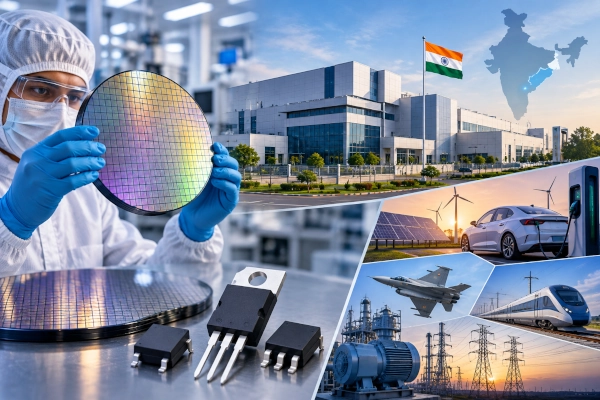
India’s effort to move beyond conventional silicon semiconductor manufacturing into advanced compound semiconductors has taken another step forward, with SiCSem Private Limited receiving Special Economic Zone approval for its planned silicon-carbide semiconductor facility in Odisha.
The Unit Approval Committee of the Falta Special Economic Zone has approved SiCSem’s proposal to establish the manufacturing unit at IDCO Infovalley-II in Arisol Mouza, Jatni Tahasil of Khordha district. The project will involve an investment of ₹3,406.25 crore, cover 21.889 acres and employ approximately 1,270 people.
Unlike many semiconductor projects centred on assembly and packaging, the SiCSem facility is intended to manufacture silicon-carbide semiconductor devices, including SiC diodes and SiC MOSFETs. The government had previously identified the project as India’s first commercial compound-semiconductor fabrication facility, giving it strategic significance within the country’s expanding semiconductor programme.
Capacity for Nearly 100 Million SiC Devices a Year
According to the Ministry of Commerce and Industry, the Odisha plant is proposed to manufacture 4.8 million silicon-carbide diodes and 91.2 million silicon-carbide MOSFETs annually.
Together, that represents production capacity of 96 million finished SiC devices every year. The project is also expected to generate approximately ₹7,043 crore in export turnover during its first five years, with projected net foreign-exchange earnings of around ₹4,523 crore over the same period.
The export projections are significant because they indicate that the plant is being designed not merely to substitute semiconductor imports for the domestic market but also to participate in international power-semiconductor supply chains.
SiCSem’s facility will operate under the jurisdiction of the Falta Special Economic Zone, giving the project an explicitly export-oriented dimension alongside its role in strengthening India’s domestic semiconductor manufacturing base.
Project Investment Has Expanded Since Cabinet Approval
The SiCSem project itself is not new. The Union Cabinet approved the proposal under the India Semiconductor Mission in August 2025, when its planned investment was stated at approximately ₹2,066 crore. At that stage, the government said the plant would have fabrication capacity of 60,000 silicon-carbide wafers annually and packaging capacity of 96 million devices a year.
The latest Falta SEZ approval places the total project cost at ₹3,406.25 crore. The current official announcement does not provide a detailed explanation for the increase from the earlier ₹2,066-crore estimate, but it establishes the larger figure as the investment associated with the project at the present approval stage.
The finished-device capacity disclosed in the new approval remains consistent with the earlier plan. The annual output of 4.8 million diodes and 91.2 million MOSFETs together corresponds to the previously announced packaging capacity of 96 million units annually.
The progression from Union Cabinet approval under the India Semiconductor Mission to SEZ unit approval is therefore important. It represents another regulatory and implementation milestone as the project moves towards establishment of the manufacturing facility.
What Makes Silicon Carbide Different From Ordinary Silicon?
Most semiconductor chips are built using silicon, but silicon carbide belongs to a class of materials known as wide-bandgap semiconductors.
Silicon carbide combines silicon and carbon in a crystalline semiconductor material whose electrical properties make it particularly valuable for managing large amounts of electrical power.
Compared with conventional silicon devices, wide-bandgap semiconductors such as SiC can operate at higher voltages, higher switching frequencies and higher temperatures while allowing power-electronic systems to become smaller and more efficient. The US Department of Energy identifies these characteristics as major advantages of silicon carbide and gallium nitride over conventional silicon in advanced power electronics.
This does not mean silicon carbide will replace ordinary silicon throughout electronics. Silicon remains exceptionally efficient and economical for processors, memory, controllers and millions of other low- and medium-power applications.
SiC becomes especially valuable when electricity has to be switched or converted efficiently under demanding conditions.
That distinction explains why the technology is increasingly important to electric vehicles, fast chargers, renewable-energy systems, industrial motor drives, railways, defence equipment and high-power electrical infrastructure.
What Are SiC MOSFETs?
A MOSFET — Metal-Oxide-Semiconductor Field-Effect Transistor — is essentially a high-speed electronic switch.
In power electronics, MOSFETs can switch electrical current thousands or even millions of times every second. By precisely controlling this switching, power-conversion systems can change voltage, convert direct current into alternating current or regulate power delivered to motors and batteries.
In an electric vehicle, for example, semiconductor switches within the traction inverter control the flow of electricity from the battery to the electric motor.
Every time that power is converted or switched, some electricity is lost as heat.
Silicon-carbide MOSFETs can reduce those switching and conduction losses in appropriate high-voltage applications. They can also operate at higher switching frequencies, allowing surrounding components such as inductors, capacitors and cooling systems to be made smaller.
This combination is why SiC devices have become increasingly important in EV powertrains and fast-charging infrastructure.
The same characteristics are valuable in solar inverters, industrial power supplies, railway traction systems and data-centre power equipment.
SiC Diodes Perform Another Critical Function
The second major product planned at the Odisha facility is the silicon-carbide diode.
A diode allows electrical current to flow primarily in one direction. Although conceptually simple, power diodes are essential components in rectifiers, power supplies, inverters, chargers and numerous other electrical systems.
SiC diodes can switch quickly while limiting some of the losses encountered in conventional silicon devices, making them particularly useful in high-frequency and high-efficiency power converters.
The planned combination of SiC MOSFET and diode manufacturing therefore positions SiCSem within the power-electronics segment of the semiconductor industry rather than the processor or memory-chip market.
From Electric Vehicles to Missiles
The applications identified by the Government of India illustrate the breadth of the market being targeted.
When approving the SiCSem project in 2025, the Union Cabinet said its devices could be used in missiles, defence equipment, electric vehicles, railways, fast chargers, data-centre racks, consumer appliances and solar-power inverters.
Many of these systems share the same fundamental requirement: they need to control large amounts of electricity efficiently while keeping power losses and thermal loads within manageable limits.
In an electric vehicle, improved power conversion can contribute to greater efficiency and potentially reduce cooling requirements. In fast chargers, SiC devices can support compact high-power conversion equipment.
In renewable energy, power semiconductors sit between sources such as photovoltaic panels and the electrical grid. Solar generation therefore requires large numbers of semiconductor switches and diodes within inverter systems.
Railway traction and industrial motor drives present another high-power application, while defence and aerospace systems can require semiconductor devices capable of operating reliably under demanding electrical and thermal conditions.
The strategic value of SiC manufacturing consequently extends across civilian, industrial and defence sectors.
India Is Moving Beyond Semiconductor Packaging
The SiCSem project is also important because India’s semiconductor programme is gradually becoming more technologically diverse.
Some of the first investments approved under the India Semiconductor Mission concentrated on semiconductor assembly, testing, marking and packaging. These operations are essential parts of the semiconductor value chain but occur after the wafer fabrication stage.
SiCSem moves India further upstream.
The Union Cabinet described the Odisha project as an integrated silicon-carbide compound-semiconductor facility and identified it as the country’s first commercial compound fab. The original project plan envisaged fabrication capacity of 5,000 wafers per month, equivalent to 60,000 wafers annually, together with packaging capacity of eight million devices per month.
That means semiconductor wafers would not simply arrive from overseas for packaging. The project is designed to establish domestic fabrication capability for the SiC devices themselves.
For India, that represents an important technological distinction.
UK Technology Partnership for the SiC Fab
SiCSem is developing the fabrication facility with technology support from Clas-SiC Wafer Fab Ltd of the United Kingdom.
When the project received Cabinet approval, the government identified Clas-SiC as SiCSem’s technology partner for the SiC fabrication component. Continental Device India Limited, or CDIL, was identified as a partner for semiconductor packaging.
The partnership is intended to help establish fabrication processes domestically while connecting the Odisha project with companies already experienced in compound-semiconductor manufacturing.
SiCSem has also been working with IIT Bhubaneswar on an even more fundamental part of the silicon-carbide supply chain.
In June 2024, SiCSem and IIT Bhubaneswar signed an agreement for compound-semiconductor research, beginning with a project aimed at indigenising SiC crystal growth. The approximately ₹45-crore research programme was designed to develop know-how for high-volume production of 150-mm and 200-mm silicon-carbide wafers.
That work is particularly important because mastering the semiconductor fabrication process is only one part of achieving technological independence. Producing high-quality SiC substrates and wafers is itself a difficult manufacturing capability.
Why SiC Wafer Technology Matters
A semiconductor fabrication plant ultimately depends on the quality of the wafer on which devices are manufactured.
Growing large, high-quality silicon-carbide crystals is considerably more difficult than producing conventional silicon wafers. Crystal defects can affect the yield and reliability of devices fabricated on them, particularly when those devices are expected to carry high voltages and currents.
If India develops domestic capabilities in SiC crystal growth, wafer preparation, device fabrication, packaging and testing, it would create a much deeper supply chain than one based solely on importing wafers and processing them locally.
The IIT Bhubaneswar collaboration therefore complements the commercial SiCSem fab by addressing technology further upstream in the manufacturing process.
Odisha Is Building a Semiconductor Cluster
SiCSem is not the only semiconductor project planned for Odisha.
In the same August 2025 Cabinet decision, the Centre approved a facility by 3D Glass Solutions in the state with an investment of approximately ₹1,943 crore. That project focuses on advanced semiconductor packaging, including glass substrates, silicon bridges and three-dimensional heterogeneous integration.
The two projects are technologically different but complementary.
SiCSem brings compound-semiconductor fabrication and power devices, while 3D Glass Solutions introduces advanced packaging and heterogeneous-integration capabilities. Concentrating these activities around the Bhubaneswar-Khordha technology corridor gives Odisha the beginnings of a semiconductor manufacturing ecosystem rather than a single isolated plant.
The state’s access to technical institutions, industrial infrastructure and an emerging electronics base could become increasingly important if suppliers, materials companies, equipment providers and design firms begin locating around the anchor projects.
Export Ambition Adds Another Dimension
The latest SEZ approval also makes clear that SiCSem is being developed with substantial international sales in mind.
The government expects the plant to generate ₹7,043 crore in exports during its first five years, producing approximately ₹4,523 crore in net foreign-exchange earnings.
That export orientation matters because the global semiconductor industry operates through highly specialised international supply chains. Even countries with substantial domestic semiconductor industries import some categories of chips while exporting others in which their manufacturers have developed specialised capabilities.
India therefore does not need to manufacture every semiconductor domestically to become an important semiconductor producer.
Developing internationally competitive specialisations such as silicon-carbide power devices could offer another route into the global value chain.
From Silicon to Compound Semiconductors
India’s semiconductor programme is now broadening beyond its initial emphasis on conventional silicon fabrication and chip packaging.
Silicon carbide represents a different technological segment, one increasingly important as the world electrifies transport, expands renewable power, constructs larger data centres and demands more efficient conversion of electricity.
The SiCSem project sits directly at that intersection.Bengaluru’s Kerael Robotics Develops Indigenous Propulsion for Heavy-Lift UAV Platform Targeting 2,500-kg Payloads
Its planned annual output of 96 million SiC devices, domestic fabrication capability, collaboration on SiC wafer technology and applications extending from EVs and solar inverters to defence equipment make it considerably more significant than its investment value alone suggests.
The latest ₹3,406.25-crore SEZ approval does not mark the beginning of the project; that began with research partnerships and was followed by Union Cabinet approval under the India Semiconductor Mission in August 2025. Instead, it marks another important step towards converting India’s first planned commercial SiC compound-semiconductor fab from an approved proposal into a manufacturing facility.
You may also like
-
Four ICAR-Developed Potato Varieties Account for Nearly 75% of India’s Cultivation Area
-
JSW Steel’s Crude Steel Production Rises 5% to 7.27 Million Tonnes in Q2 FY2027
-
Jubilant Pharmova Announces CAD 94.5 Million Expansion of Canadian Radiopharmaceutical Facility
-
Kabra Extrusiontechnik’s GEON Commissions 20 MWh Battery Storage Project in Rajasthan
-
OBSC Perfection Secures ₹8.9 Crore Israeli Defence Order for Precision Fuze Components
