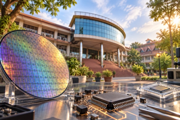
National Institute of Technology Calicut is building a growing presence in India’s semiconductor design ecosystem, with its researchers moving beyond simulation and circuit design into the more demanding stage of fabricated silicon. Official records under the Ministry of Electronics and Information Technology’s Chips to Startup programme show multiple NIT Calicut integrated-circuit designs progressing through the national chip fabrication pipeline, while earlier designs from the institute have already been fabricated at the Semiconductor Laboratory in Mohali.
The development places NIT Calicut within a much wider national effort to give universities access to semiconductor design tools, fabrication facilities and packaging infrastructure that would otherwise be prohibitively expensive for individual institutions. Through the C2S programme and the ChipIN Centre, academic researchers can now take a circuit from schematic and layout through verification, tape-out, fabrication and eventually silicon testing.
Programmable Gain Amplifier Moves Into the Fabrication Pipeline
One of NIT Calicut’s recent designs is a Programmable Gain Amplifier, identified in the official C2S records by silicon number C2S0047. The design was submitted through the ChipIN Centre as part of MPW Shuttle-II for fabrication at the Semiconductor Laboratory in Mohali using its 180-nanometre process technology.
A programmable gain amplifier is an analog circuit whose amplification can be electronically adjusted according to the strength of the incoming signal. Such circuits are widely used in sensor interfaces, instrumentation systems, communication equipment and mixed-signal electronics, where signals arriving from sensors or other analog sources may vary significantly in amplitude.
The significance of the project lies not only in the function of the amplifier but also in the process through which the design is being taken towards silicon. Designing a circuit on a computer is only one stage of semiconductor development. The design must satisfy fabrication rules, pass verification and be converted into a physical layout that can be manufactured reliably on a semiconductor wafer.
A Second Design Targets Real-Time Traction Control
NIT Calicut also appears in the C2S MPW Shuttle-III records with a real-time traction control system, carrying silicon number C2S0095. This design was submitted for fabrication through the ChipIN Centre using the same SCL Mohali 180 nm technology platform.
The official C2S listing does not disclose the detailed internal architecture, performance parameters or intended vehicle platform of the NIT Calicut design. It should therefore not yet be described as a production automotive chip. What is officially established is that the institute submitted a real-time traction-control integrated-circuit design into the national fabrication programme.
Traction-control electronics operate within demanding real-time environments because they must react quickly to changing wheel and drivetrain conditions. Bringing such control functions into dedicated silicon can offer advantages in speed, determinism, power consumption and integration compared with implementing every function through general-purpose computing hardware.
The project also shows the range of work emerging from university semiconductor programmes. NIT Calicut’s C2S activity is not confined to a single analog circuit but extends into real-time control applications with potential relevance to automotive and embedded systems.
NIT Calicut Has Already Reached Fabricated Silicon
The institute’s semiconductor experience predates these two recent submissions. The official C2S database of ASICs fabricated at SCL Mohali lists multiple NIT Calicut designs manufactured using the 180 nm process.
These include an OTA buffer, a clock generator, an OTA-based high-speed buffer for line drivers and a PLL-based clock generator. Their presence in the official fabricated-ASIC list confirms that NIT Calicut has already crossed the boundary between designing integrated circuits and receiving physical silicon produced at an Indian semiconductor fabrication facility.
This is an important distinction in semiconductor education and research. A circuit that performs well in simulation may behave differently after fabrication because of process variations, parasitic effects, temperature, noise and other physical factors. Receiving fabricated silicon allows researchers to test whether theoretical and simulated performance survives the transition to a real chip.
From Design File to Physical Chip
The route from an academic design laboratory to SCL Mohali is being enabled by the ChipIN Centre at C-DAC Bengaluru. The facility acts as a national semiconductor design hub under the C2S programme, providing participating institutions with access to commercial Electronic Design Automation tools, high-performance computing, semiconductor IP libraries and technical support.
ChipIN also performs an important role between the designers and the fabrication plant. Designs submitted by universities are checked for compliance with manufacturing requirements, and researchers may have to revise layouts before the circuits are accepted for tape-out.
Several designs from different institutions are then combined into a single Multi-Project Wafer, or MPW, run. Instead of manufacturing a separate wafer for every university circuit, multiple designs share the same fabrication run. This dramatically reduces the cost of producing small quantities of experimental chips.
SCL Mohali then fabricates the designs, after which approved chips can be packaged and returned to the institutions for testing.
Why 180 nm Is Well Suited to Analog and Control Chips
The 180 nm process used for these academic fabrication runs is not at the leading edge of commercial processor manufacturing, where substantially smaller technology nodes are used. That does not make it obsolete for the type of work being undertaken by universities.
Analog circuits, sensor interfaces, control electronics, power-management systems and many embedded applications do not necessarily require the smallest available transistor geometries. Mature nodes can offer lower development costs, easier design access and proven manufacturing characteristics.
For academic institutions, the larger value lies in allowing students and researchers to experience the complete semiconductor development cycle. A researcher who has taken a design through layout, verification, tape-out, fabrication and testing gains a very different understanding of chip development from someone whose work ends with computer simulation.
Defence Sensor Research Adds Another Dimension
NIT Calicut is also participating in a larger C2S consortium developing High Precision Interfacing Circuits for Capacitive Based Sensors for defence applications.
The project is led by IIT Hyderabad and includes IIT Bhilai, NIT Warangal and NIT Calicut. Official C2S records identify Dr Dhanaraj K. J., Dr B. Bhuvan and Dr Ashitosh Mishra among the NIT Calicut researchers associated with the programme.
Capacitive sensors are used in applications where small changes in displacement, pressure, acceleration or other physical parameters have to be converted into measurable electrical signals. The quality of the electronic interface becomes particularly important when the sensor signal is extremely small or must be measured with high precision.
Developing indigenous interface circuits for such sensors has relevance beyond academic research because precision sensing is important across aerospace, defence, navigation, industrial control and instrumentation.
Semiconductor Capability Is Being Built Inside Universities
The larger significance of NIT Calicut’s work becomes clearer when viewed alongside the national C2S programme.
The programme was launched by MeitY in 2022 with an outlay of ₹250 crore over five years and a target of developing 85,000 industry-ready professionals across undergraduate, postgraduate and doctoral levels. It is intended to provide academic institutions with access to semiconductor design infrastructure that few universities could afford independently.
By January 2026, more than one lakh individuals had enrolled in chip-design training, with approximately 67,000 already trained. The ChipIN Centre had conducted six shared wafer runs, while SCL Mohali had received 122 submissions from 46 institutions. Fifty-six student-designed chips had already been successfully fabricated, packaged and delivered.
By April 2026, the wider academic ecosystem had produced 211 tape-outs from 75 institutions, showing how semiconductor design activity was spreading beyond a small group of traditional chip-design centres.
NIT Calicut’s participation is part of this broader attempt to distribute semiconductor expertise across Indian universities.
Tape-Out Is a Major Milestone, but Not the Final Step
The semiconductor industry uses the term tape-out for the point at which a completed design is released for fabrication. It represents a major milestone because the schematic, physical layout and verification process must be completed before the design can be sent to the foundry.
Tape-out, however, does not automatically mean that a finished chip has been successfully fabricated and validated.
After fabrication, the silicon must be packaged and tested. Researchers then compare the actual measurements with the expected performance from simulations. Problems discovered at this stage may require design changes followed by another fabrication cycle.
This distinction matters when describing NIT Calicut’s recent work. The official records clearly establish the PGA and traction-control system as designs submitted into MPW fabrication shuttles, while the C2S database separately confirms earlier NIT Calicut designs that have already been fabricated.
Building Engineers Who Understand Silicon
India’s semiconductor ambitions require more than fabrication plants. They require engineers who understand how a semiconductor product moves from an idea to a physical device.
That includes architecture, circuit design, verification, physical layout, process-design rules, fabrication constraints, packaging and post-silicon testing. Engineers with experience across these stages are essential for both domestic semiconductor companies and international firms expanding engineering and manufacturing activity in India.
Programmes such as C2S are therefore designed as much around human capability as around individual chips. A university chip may never become a mass-market commercial product, but the engineers who design and test it acquire skills that can later be applied to industrial semiconductor programmes.
For institutions such as NIT Calicut, access to real fabrication changes the character of VLSI education from primarily theoretical instruction into practical semiconductor engineering.
NIT Calicut Builds on an Existing VLSI Foundation
NIT Calicut’s participation in national semiconductor programmes also builds on an older foundation in VLSI education and research. The institute was part of earlier national programmes that established VLSI design laboratories, provided Electronic Design Automation tools and supported specialised semiconductor training.
Government records from earlier semiconductor manpower-development programmes show NIT Calicut among the participating institutions developing VLSI expertise. The current C2S programme represents the next stage of that journey because researchers are gaining routine access not only to design tools but also to national fabrication infrastructure.
The progression from VLSI laboratories to tape-outs and fabricated ASICs demonstrates how long-term academic capacity-building can eventually produce practical semiconductor capability.
Kerala’s Role in India’s Semiconductor Talent Pipeline
NIT Calicut’s work is also significant for Kerala because semiconductor activity in India is no longer restricted to a few metropolitan technology clusters.
Kerala already possesses a large engineering education base and a growing electronics and technology ecosystem. University-level experience with actual chip fabrication can strengthen the pipeline of engineers available for semiconductor design, embedded systems and electronics companies.
Other institutions in the state are also participating in semiconductor and electronics programmes, creating the possibility of a broader regional design ecosystem rather than isolated academic projects.
NIT Calicut’s chip-development work therefore has implications beyond the institute itself. Every successful tape-out, fabricated ASIC and trained researcher adds depth to the semiconductor talent pool available within the state and the country.
From Academic Circuit Design to Indian Silicon
The most important aspect of NIT Calicut’s semiconductor work is the transition from theoretical design towards physical silicon.
The institute already has multiple ASIC designs listed as fabricated at SCL Mohali. Its newer Programmable Gain Amplifier and real-time traction-control system have entered the C2S fabrication pipeline, while its researchers are participating in a defence-oriented precision sensor-interface programme.
None of these projects alone will determine India’s semiconductor future. Their importance lies in what they represent collectively: Indian students and researchers are increasingly gaining experience across the complete chip-development process rather than remaining confined to simulation and classroom instruction.
India’s semiconductor ambitions will ultimately depend on fabrication plants, equipment manufacturers, materials suppliers, design companies and substantial private investment. They will also depend on thousands of engineers who understand how to turn an electronic circuit into functioning silicon.
At NIT Calicut, that transition has already begun.
References
Ministry of Electronics and Information Technology — Chips to Startup Programme, MPW Shuttle-II
https://c2s.gov.in/MPW-II_through_ChipIN.jsp
Ministry of Electronics and Information Technology — Chips to Startup Programme, MPW Shuttle-III
https://c2s.gov.in/MPW-III_through_ChipIN.jsp
Chips to Startup Programme — ASICs Fabricated at SCL Mohali
https://c2s.gov.in/asics_fabricated.jsp
Chips to Startup Programme — Consolidated MPW Shuttle Records
https://c2s.gov.in/MPW_Shuttles_through_ChipIN_Consolidated.jsp
Chips to Startup Programme — Selected Research Proposals
https://c2s.gov.in/proposallist.jsp
Press Information Bureau — Chips to Startup Programme: Fostering India’s Indigenous Chip Design Ecosystem, 18 January 2026
https://www.pib.gov.in/PressReleasePage.aspx?PRID=2215755
Ministry of Electronics and Information Technology / PIB — C2S Semiconductor Talent Development, 7 March 2026
https://www.pib.gov.in/PressReleasePage.aspx?PRID=2236290
Ministry of Electronics and Information Technology / PIB — Government Democratising Chip Design Through EDA Tools and MPW Fabrication, 29 November 2025
https://www.pib.gov.in/PressReleasePage.aspx?PRID=2196422
Ministry of Electronics and Information Technology / PIB — Semicon India 2026 and India’s Expanding Chip Design Ecosystem
https://www.pib.gov.in/FeaturesDeatils.aspx?ModuleId=2&NoteId=159979
You may also like
-
India’s Economic Warfare Challenge: Strategic Autonomy, Energy Security and the Rise of a Global Power
-
India-US Trade Deal Stalemate: Why Washington’s Tariff Pressure Has Failed to Secure an Agreement
-
US Double Standards in Foreign Policy: 16 Recent Cases Involving India, Russia, China and Global Trade
-
India’s Arctic Energy Ambitions: Russian Oil, LNG and a New Sea Route to Indian Ports
-
India and Russia Explore Joint Icebreaker Construction as Maritime Industrial Cooperation Expands
