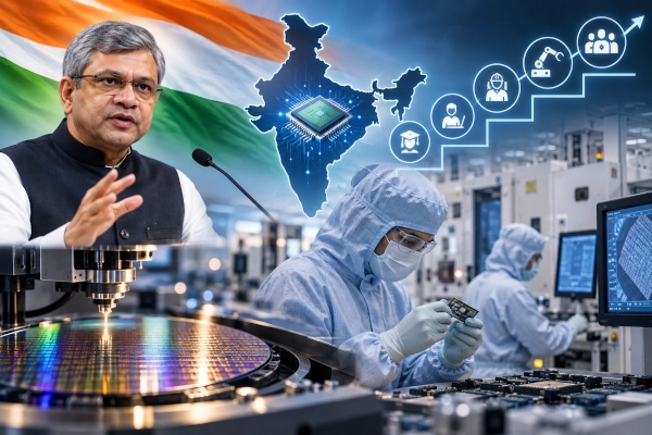
India is preparing to establish its first dedicated Precision Manufacturing Institute under the broader Semicon 2.0 programme, with the aim of creating a skilled workforce for semiconductor manufacturing, equipment production and advanced precision engineering. The initiative is intended to address a growing need for technicians and manufacturing specialists as India’s semiconductor projects move from construction and design activity towards large-scale industrial production.
Electronics and Information Technology Minister Ashwini Vaishnaw outlined the proposal during SEMICON India 2026, saying that the institute would be built around a five-level skilling model. The government wants the training framework to extend beyond conventional chip design and include systems engineering, precision manufacturing, semiconductor production and equipment-related skills.
The proposal reflects the wider direction of Semicon 2.0, which is attempting to build a complete semiconductor ecosystem rather than focusing only on fabrication plants. As new fabs, packaging facilities and semiconductor suppliers begin operations in India, the demand for trained personnel capable of working in highly controlled manufacturing environments is expected to rise significantly.
Precision Manufacturing Institute to Address a Major Skills Gap
The proposed institute is intended to address one of the most important challenges facing India’s semiconductor expansion: the shortage of workers trained specifically for advanced manufacturing environments.
Semiconductor fabs and packaging plants require a large technical workforce in addition to chip designers and electronics engineers. These facilities depend on personnel capable of operating cleanrooms, maintaining equipment, handling ultra-pure chemicals and gases, monitoring production lines and supporting strict process-control standards.
As manufacturing activity increases, the requirement for skilled technicians will grow alongside the need for engineers. The Precision Manufacturing Institute is intended to create a structured training pathway for these industrial roles rather than relying only on conventional engineering education.
Five-Level Skilling Model Planned
The government plans to organise the institute around a five-level skilling framework that can accommodate trainees with different educational backgrounds and progressively build more advanced capabilities.
The first level is expected to involve around 240 hours of training and could be accessible to students entering directly from school. Higher levels would then introduce increasingly specialised technical content, allowing trainees to progress towards more advanced roles in semiconductor manufacturing and precision engineering.
This approach is important because many jobs in semiconductor factories do not necessarily require a four-year engineering degree. Cleanroom operators, equipment technicians, maintenance specialists and process-support personnel need substantial technical training, but much of that capability can be developed through focused vocational and diploma-level programmes.
A multi-level model could therefore broaden access to semiconductor employment while giving companies a more reliable source of job-ready manufacturing personnel.
Training to Expand Beyond Chip Design
India’s semiconductor talent programmes have so far placed considerable emphasis on chip design, electronic design automation and semiconductor engineering. Under Semicon 2.0, the government intends to widen this focus towards systems design, manufacturing and precision engineering.
The objective is to build a workforce that understands not only how semiconductor devices are designed, but also how they are produced, packaged, tested and integrated into complete electronic systems.
This is an important transition because semiconductor manufacturing requires capabilities across the entire value chain. Strong chip-design skills alone are not sufficient if factories lack trained personnel to operate equipment, maintain production quality and support high-volume manufacturing.
India already has a large pool of semiconductor design engineers. The next stage is to develop comparable depth in manufacturing and industrial execution.
One Lakh Technicians Targeted Under Semicon 2.0
The government is targeting the training of approximately one lakh technicians under the expanded semiconductor programme.
These workers are expected to support semiconductor fabrication, ATMP and OSAT operations, advanced packaging, equipment manufacturing and related precision-engineering industries.
The scale of the target reflects the number of semiconductor projects now being developed across India. As these facilities move towards commercial production, companies will need trained personnel capable of operating machinery continuously, maintaining cleanroom conditions and supporting highly automated manufacturing processes.
Developing this workforce in advance could help prevent a situation in which new semiconductor factories face delays because suitable technicians are unavailable.
Semiconductor Manufacturing Requires Exceptional Precision
Semiconductor manufacturing operates at levels of accuracy that are far beyond most conventional industrial environments. Equipment components must be produced and assembled to extremely tight tolerances, while wafer-processing facilities must control dust, moisture, temperature and contamination at microscopic levels.
A modern semiconductor fab relies on vacuum systems, precision robotics, gas-delivery equipment, valves, pumps, temperature-control systems and sophisticated automation. Maintaining these systems requires technicians trained in electronics, mechatronics, instrumentation, mechanical systems and process control.
A dedicated Precision Manufacturing Institute could help standardise this type of training while ensuring that the curriculum remains aligned with the actual needs of semiconductor companies.
Equipment Manufacturing Creates a New Industrial Opportunity
Semicon 2.0 also gives greater importance to semiconductor manufacturing equipment and the specialised components used within it.
India is unlikely to manufacture every advanced semiconductor tool domestically in the near term, but there are significant opportunities to localise components, subassemblies and supporting systems.
Indian companies already possess capabilities in precision machining, aerospace manufacturing, industrial automation and defence engineering that could potentially be adapted to semiconductor applications.
Components such as vacuum chambers, gas systems, precision mechanical assemblies, valves, pumps and specialised tooling could eventually form part of a domestic semiconductor equipment supply chain.
The workforce trained through the proposed institute could support this emerging industrial opportunity.
Precision Skills Could Benefit Aerospace and Defence
Many of the skills required for semiconductor manufacturing overlap with capabilities needed in aerospace, defence, medical technology and other advanced engineering sectors.
These industries all depend on tight tolerances, sophisticated materials, strict quality control and high-reliability production processes.
A workforce trained to semiconductor manufacturing standards could therefore have value well beyond the chip industry.
Indian companies that already work in aerospace or defence precision manufacturing may also find opportunities to diversify into semiconductor equipment, tooling and component production.
The Precision Manufacturing Institute could help create the trained workforce needed to support this crossover between advanced industries.
Workforce Development Becomes Central to Semiconductor Growth
The expansion of India’s semiconductor sector has made workforce development a central policy priority rather than a secondary issue.
SEMICON India 2026 has also placed emphasis on career development, training pathways and industry-academia interaction. The broader objective is to ensure that India’s semiconductor growth is supported by a workforce capable of handling both engineering and manufacturing roles.
This is particularly important because the industry requires a wide range of skills. Advanced research and chip design may require highly specialised engineers, while manufacturing plants need technicians, operators, equipment specialists and quality-control personnel in much larger numbers.
The proposed institute is intended to support this broader talent structure.
From Semiconductor Engineers to an Industrial Workforce
India already produces large numbers of electronics, electrical and computer-science engineers and has built a strong reputation in semiconductor design.
Manufacturing, however, requires a different type of workforce.
A large semiconductor facility may employ process engineers and equipment specialists, but it also depends on thousands of technicians and operators who keep production running around the clock.
This creates demand for vocational, diploma-level and practical industrial training alongside university engineering programmes.
The five-level skilling model proposed for the Precision Manufacturing Institute is intended to create pathways for workers to enter the industry at different levels and progressively develop more advanced capabilities.
India Seeks a Complete Semiconductor Talent Pipeline
The broader objective of Semicon 2.0 is to create a workforce covering every stage of the semiconductor value chain.
At one end are chip architects, circuit designers and researchers. At the other are process technicians, equipment operators, packaging specialists and precision-manufacturing workers responsible for keeping production lines operating efficiently.
Between these groups are manufacturing engineers, systems engineers, test specialists and equipment experts who connect design with physical production.
A complete semiconductor ecosystem needs all of these roles to function together. The proposed institute is therefore part of a wider effort to ensure that India’s semiconductor ambitions are matched by the workforce required to support them.
A Critical Step Towards Semiconductor Industrialisation
The proposed Precision Manufacturing Institute represents an important shift in India’s semiconductor workforce strategy.
Building fabs and advanced packaging facilities requires massive capital investment, but these plants cannot operate effectively without trained people capable of working in highly precise industrial environments.
By introducing a five-level skilling model and broadening training from chip design towards systems engineering and precision manufacturing, the government is attempting to prepare the workforce before semiconductor production reaches much larger scale.
The benefits could also extend into aerospace, defence, electronics and other advanced industries, giving the initiative significance beyond the semiconductor sector itself.
References
- ThePrint — India to Set Up First Precision Manufacturing Institute With Five-Level Skilling Model, Vaishnaw at SEMICON, 18 September 2026
https://theprint.in/tech/india-to-set-up-1st-precision-manufacturing-institute-with-5-level-skilling-model-vaishnaw-at-semicon/3046745/ - Press Information Bureau, Ministry of Electronics & Information Technology — Semicon 2.0 to Deepen India’s Semiconductor Ecosystem With Focus on Design, Equipment, Fabs, Advanced Packaging, R&D and Talent, 17 September 2026
https://www.pib.gov.in/PressReleseDetailm.aspx?PRID=2311630 - SEMICON India 2026 — Workforce Development Pavilion
https://www.semiconindia.org/special-features-2026/Workforce-pavilion - SEMICON India 2026 — SEMI University Training Programme: Semiconductor Manufacturing — From Wafer to Chip, 18 September 2026
https://www.semiconindia.org/special-features-2026/semi-u - SEMICON India 2026 — Event Overview
https://www.semiconindia.org/about/overview
You may also like
-
Nayan Technologies Selected by JSW MG Motor to Advance AI-Based Road Monitoring and Smart Mobility
-
From ‘We Will Coup Whoever We Want’ to Starlink in India: Elon Musk, Corporate Pressure and National Sovereignty
-
Indian Navy to Commission Indigenous Anti-Submarine Warfare Ship Mangrol on October 12
-
Starlink-Ukraine, Myanmar and Drug Smuggling: Why India Must Regulate Satellite Internet for National Security
-
Four ICAR-Developed Potato Varieties Account for Nearly 75% of India’s Cultivation Area
