HCLTech Opens ₹185-Crore Semiconductor Testing and Engineering Hub in Bengaluru
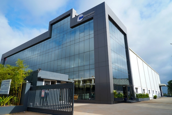
The 40,000-square-foot facility includes 25,000 square feet of Class 10K and Class 1K cleanrooms and is designed to handle semiconductor validation, automated testing, reliability qualification and failure analysis after a chip has been manufactured. HCLTech formally announced the facility on September 8.