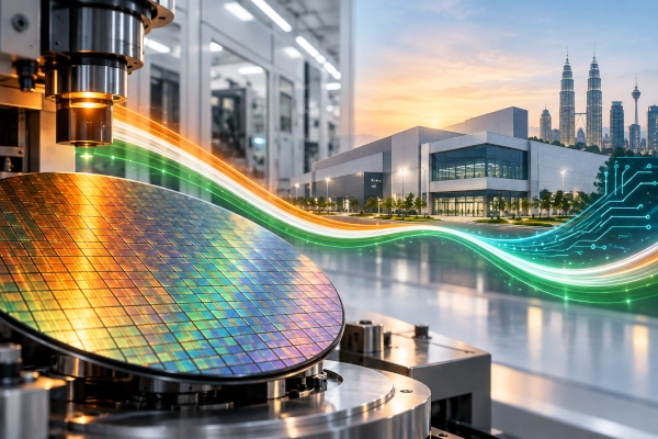
India–Malaysia semiconductor cooperation has moved from discussions and industry exchanges into a major manufacturing project, with Tata Electronics bringing Malaysian engineering specialist Kelington Group into the development of its semiconductor fabrication facility at Dholera in Gujarat.
The collaboration will place Kelington’s semiconductor infrastructure expertise inside one of India’s most important technology projects. Tata Electronics is developing the Dholera facility as a 300-mm, or 12-inch, wafer fabrication plant with a planned investment of around $11 billion.
The partnership was announced on 18 September 2026 during SEMICON India 2026 in New Delhi. Kelington will support the deployment of critical infrastructure and systems required to prepare the fab for silicon-wafer production.
Kelington to Support Critical Fab Infrastructure
A semiconductor fabrication plant requires far more than chipmaking equipment. Each production tool must be connected to precisely controlled supplies of high-purity gases, chemicals, water, vacuum systems and other utilities while maintaining exceptionally strict standards of cleanliness and safety.
Kelington specialises in this part of the semiconductor manufacturing chain. Its work includes ultra-high-purity systems, process piping, gas distribution and engineering required to connect production equipment with the infrastructure of a semiconductor fab.
For Tata Electronics, this expertise is particularly important as construction at Dholera moves towards operational readiness. Tool hook-up is one of the critical stages between installing semiconductor equipment and bringing a fabrication line into production.
Tata Electronics Chief Executive and Managing Director Randhir Thakur described tool hook-up as essential to creating a reliable and efficient fab environment capable of integrating highly sophisticated production equipment from the beginning.
Dholera Fab Moves Closer to Wafer Production
The Dholera project forms the centrepiece of Tata Electronics’ semiconductor manufacturing programme.
The plant is being designed as a 12-inch wafer fabrication facility capable of producing semiconductor products for applications including automobiles, mobile devices and artificial intelligence. Its output is intended for both Indian and international customers.
The project represents one of the largest individual investments in India’s emerging semiconductor industry and is central to the country’s attempt to establish domestic front-end chip manufacturing rather than remaining concentrated primarily in design, electronics assembly and semiconductor packaging.
Moving from construction to actual wafer manufacturing requires hundreds of specialised suppliers. Tata Electronics has indicated that its Dholera ecosystem already involves around 450 suppliers, illustrating the complexity of building a modern fabrication facility.
Malaysia Brings Decades of Semiconductor Experience
Kelington’s participation also highlights Malaysia’s growing relevance to India’s semiconductor strategy.
Malaysia has been part of the global semiconductor supply chain for several decades and has developed substantial capabilities in semiconductor assembly, testing, packaging, equipment support, engineering services and specialised manufacturing infrastructure.
Companies operating in Malaysia support many of the world’s major semiconductor manufacturers, giving the country an established industrial base that India can draw upon as it builds fabs and advanced packaging facilities of its own.
The Tata–Kelington agreement therefore represents more than a conventional engineering contract. It connects India’s expanding fabrication programme with an experienced Southeast Asian semiconductor ecosystem.
Local Engineering Capability Part of the Partnership
The collaboration is also expected to extend beyond physical construction.
Tata Electronics and Kelington said they will explore the development of local talent and advanced design-and-build engineering capabilities in India.
This is important because semiconductor manufacturing requires specialised engineering skills that are still relatively scarce in India. Building fabs without simultaneously developing engineers and technicians capable of operating and maintaining them would leave the domestic ecosystem dependent on overseas expertise.
Participation by experienced semiconductor engineering firms gives Indian teams the opportunity to develop practical skills in areas such as high-purity systems, facility engineering, equipment integration and fab operations.
Malaysia Had Strong Presence at SEMICON India 2026
The agreement came during a SEMICON India event that featured significant Malaysian participation.
Malaysia was among the six countries with dedicated national pavilions at SEMICON India 2026, alongside Japan, South Korea, Singapore, the Netherlands and Sweden. The three-day event brought together more than 600 exhibitors, including around 300 international participants, with representatives from 52 countries.
Malaysia’s participation reflected growing interest in connecting its established semiconductor manufacturing ecosystem with India’s expanding market and new manufacturing projects.
The event produced 56 MoUs, announcements and strategic initiatives across semiconductor design, fabrication, advanced packaging, materials, equipment, research, startups and workforce development.
Dholera Is Becoming a Semiconductor Supply-Chain Cluster
The Kelington agreement is one of several partnerships being assembled around Tata Electronics’ Dholera project.
Rather than importing every component of the fab ecosystem independently, Tata Electronics is bringing specialised global companies into the project across equipment, semiconductor materials, infrastructure and manufacturing technologies.
ASML has already entered a strategic partnership with Tata Electronics to support the establishment and ramp-up of lithography capabilities at Dholera. Fujifilm has also announced plans to work with Tata Electronics on semiconductor materials and establish local manufacturing capacity around the project.
Dutch semiconductor company Nexperia is another recent partner, with plans for semiconductor products to be manufactured at Dholera and subsequently packaged and tested through Tata Electronics’ semiconductor operations in Assam.
The result is gradually transforming Dholera from a single fabrication project into a wider semiconductor manufacturing cluster.
Why High-Purity Infrastructure Matters
The infrastructure supplied to a semiconductor fab operates under standards very different from those of conventional factories.
Microscopic contamination can damage wafers containing thousands of individual chips. Gases and chemicals therefore have to reach production equipment at extremely high levels of purity, while pipelines and distribution systems must prevent contamination, leakage and unwanted chemical reactions.
Every major production tool must also be correctly integrated with these utility networks before commercial manufacturing can begin.
This makes companies specialising in high-purity semiconductor infrastructure an essential part of a fab’s construction and commissioning process.
Kelington’s role therefore sits directly between the construction of the facility and the point at which chipmaking equipment can begin producing wafers.
India Is Building the Ecosystem Around the Fab
The partnership also illustrates how India’s semiconductor strategy is changing.
The first phase of the India Semiconductor Mission focused heavily on attracting large anchor investments in fabs, assembly and packaging plants. With those projects now advancing, attention is increasingly shifting towards the companies that supply equipment, gases, chemicals, materials, precision components and engineering services.
The government’s newly announced Semicon 2.0 programme, with an outlay of ₹1,27,500 crore, is structured around six areas covering semiconductor design, machines and materials, new fabs, advanced packaging, research and talent development.
This second phase is designed to fill the gaps surrounding the large manufacturing projects already under construction.
The arrival of companies such as Kelington within the Dholera ecosystem illustrates how that transition is beginning to occur commercially.
India and Malaysia Have Complementary Semiconductor Strengths
India and Malaysia enter this emerging partnership from different positions within the semiconductor value chain.
India possesses a large semiconductor-design workforce, a rapidly expanding electronics market and a government-backed programme to establish domestic fabrication and packaging. Malaysia already has extensive experience in semiconductor manufacturing services, assembly, testing, packaging and industrial engineering.
These capabilities are complementary rather than directly competitive.
Malaysian companies can participate in India’s new fabs, packaging facilities and supplier networks, while Indian semiconductor and technology companies gain access to experienced Southeast Asian manufacturing partners and regional supply chains.
As semiconductor companies seek to diversify production geographically, stronger industrial links between India and Malaysia could become increasingly important.
A Commercial Link Between Two Asian Semiconductor Ecosystems
The Tata Electronics–Kelington collaboration is therefore significant beyond the immediate engineering work at Dholera.
It places Malaysian semiconductor expertise directly inside India’s largest emerging wafer-fabrication project and provides another example of India’s semiconductor programme drawing specialised capabilities from established Asian manufacturing centres.
For Malaysia, India’s rapid expansion creates opportunities for engineering companies, equipment suppliers, packaging specialists and semiconductor service providers.
For India, such partnerships provide something equally important: the technical knowledge and supplier ecosystem required to convert expensive fabrication plants into functioning semiconductor manufacturing centres.
As Dholera moves closer to wafer production, partnerships of this kind will determine whether India can build not merely individual chip factories, but the dense network of suppliers, engineers and specialist manufacturers required to sustain a competitive semiconductor industry.
References
Tata Electronics — Tata Electronics and Kelington Collaborate to Accelerate Operational Readiness of Dholera Fab, 18 September 2026.
BERNAMA — Tata Electronics Partners With Malaysia’s Kelington for Chip Plant in Gujarat, 19 September 2026.
Press Information Bureau, Ministry of Electronics and Information Technology — SEMICON India 2026 Concludes Successfully, 19 September 2026.
Tata Electronics — Tata Electronics and ASML Strategic Partnership, May 2026.
Press Information Bureau — Semicon 2.0 implementation framework and semiconductor ecosystem expansion, September 2026.
You may also like
-
India’s Economic Warfare Challenge: Strategic Autonomy, Energy Security and the Rise of a Global Power
-
India-US Trade Deal Stalemate: Why Washington’s Tariff Pressure Has Failed to Secure an Agreement
-
US Double Standards in Foreign Policy: 16 Recent Cases Involving India, Russia, China and Global Trade
-
India’s Arctic Energy Ambitions: Russian Oil, LNG and a New Sea Route to Indian Ports
-
India and Russia Explore Joint Icebreaker Construction as Maritime Industrial Cooperation Expands
