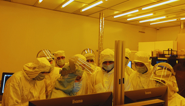
India is moving into the second phase of its semiconductor programme with a much broader industrial strategy that extends beyond fabrication plants and assembly facilities. Under Semicon 2.0, the government is targeting support for around 200 chip-design companies and startups while also preparing to train approximately one lakh technicians for semiconductor manufacturing and related industries.
The expanded programme was approved by the Union Cabinet on 15 July 2026 with a total outlay of ₹1,27,500 crore. Semicon 2.0 is built around six pillars covering semiconductor design, machines and materials, new fabrication plants, advanced packaging, research and development, and talent development. The objective is to build a more complete domestic semiconductor ecosystem rather than concentrating policy support only on fabs and ATMP or OSAT facilities.
At SEMICON India 2026, Electronics and Information Technology Minister Ashwini Vaishnaw said the second phase is intended to scale the design ecosystem, strengthen precision manufacturing and create the workforce needed to support India’s expanding semiconductor industry. The government has also reported around ₹1 lakh crore in investment commitments across the wider ecosystem, including equipment, materials and other supporting industries.
Semicon 2.0 Moves Beyond the Fab-Centred Approach
The first phase of India’s semiconductor programme concentrated heavily on establishing basic manufacturing capacity through fabs and semiconductor assembly, testing, marking and packaging projects. Semicon 2.0 expands this framework by giving greater policy attention to the supporting industries that a sustainable semiconductor manufacturing base requires.
The programme now covers the full chain from design and research to manufacturing equipment, process materials, advanced packaging and workforce development. This broader structure reflects the reality that fabrication plants cannot operate efficiently in isolation. They depend on specialised equipment suppliers, chemical and materials companies, packaging operations, design firms, precision manufacturers and trained technical personnel.
The government describes the objective as building a complete chip value chain within India while strengthening supply-chain resilience and developing high-value industrial employment.
Around 200 Chip-Design Companies and Startups Targeted
One of the central objectives of Semicon 2.0 is to expand India’s domestic chip-design ecosystem. Under Semicon 1.0, more than 100 startups had already begun developing chips with government support, providing the foundation for the next stage of the programme.
The government now wants to expand this base towards roughly 200 semiconductor design companies and startups. The emphasis is not merely on increasing the number of engineers working in chip design, but on encouraging Indian companies to develop proprietary semiconductor intellectual property and commercially viable products.
India already has a substantial semiconductor design workforce and hosts a large share of the global engineering operations of major semiconductor companies. The next challenge is to translate that engineering capability into more Indian-owned chip architectures, products and intellectual property.
Such companies could eventually develop semiconductor products for automotive systems, industrial electronics, telecommunications, defence, artificial intelligence, digital infrastructure, energy and consumer electronics.
More Than One Lakh Engineers Already Have Access to Chip-Design Tools
The government has already created a substantial base for expanding the design ecosystem. More than one lakh engineers across approximately 500 organisations have been provided access to advanced semiconductor design tools, including participants from academic institutions and startups.
Indian organisations participating in these programmes have developed hundreds of chip designs, while separate government talent-development initiatives have supported large-scale training and design activity across universities and research institutions.
Providing shared access to electronic design automation tools is particularly important for smaller companies because commercial semiconductor design software can be extremely expensive. Centralised access allows startups and universities to work on advanced chip designs without having to bear the full cost of individual licences and infrastructure.
One Lakh Semiconductor Technicians to Be Trained
Semicon 2.0 also places major emphasis on developing the workforce required to operate semiconductor manufacturing facilities. The government plans to train approximately one lakh technicians who can work across fabrication, packaging, testing, equipment maintenance and related precision-manufacturing operations.
The demand for technicians is different from the requirement for chip-design engineers. Semiconductor fabs and packaging plants require large numbers of skilled personnel who can operate cleanroom equipment, monitor production processes, maintain specialised machinery, handle sensitive materials and support quality-control systems.
As new semiconductor projects move from construction into commercial production, this category of workforce will become increasingly important. Training one lakh technicians is therefore intended to ensure that industrial expansion is not constrained by a shortage of shop-floor and process-manufacturing skills.
Semiconductor Talent Development Already Underway
India has already begun building a semiconductor workforce through multiple training programmes. By 2026, government initiatives had trained large numbers of engineers and students across chip design, manufacturing and advanced packaging.
The first phase of these programmes focused heavily on design talent, while Semicon 2.0 is intended to expand the workforce base into manufacturing, packaging and technician-level roles.
This broader approach reflects the needs of a maturing semiconductor industry. Engineers remain essential, but technicians, equipment specialists, process operators and precision-manufacturing personnel are equally important once large factories begin operating at scale.
Precision Manufacturing Becomes a Major Focus
The government is also placing greater emphasis on precision manufacturing under Semicon 2.0. Semiconductor equipment and supporting systems require extremely accurate mechanical, electrical and materials engineering, creating opportunities for Indian companies that already operate in sectors such as aerospace, defence, electronics and high-end industrial manufacturing.
Building capability in precision components, tooling, gas-delivery equipment, vacuum systems and specialised mechanical assemblies could allow Indian companies to participate in semiconductor manufacturing without necessarily building complete fabrication equipment.
This approach could also create a wider industrial spillover because the manufacturing capabilities required for semiconductor equipment overlap with those needed in aerospace, advanced electronics, medical devices and other high-technology industries.
Machines and Materials Become a Separate Strategic Pillar
Semicon 2.0 gives semiconductor machines and materials their own dedicated policy pillar. India currently imports a large proportion of the equipment, chemicals, gases and specialised materials required for chip manufacturing, making these areas critical to supply-chain resilience.
Developing selected domestic capabilities in equipment and materials could reduce dependence on overseas suppliers while opening new markets for Indian engineering companies. The government is not attempting to reproduce every part of the semiconductor supply chain domestically, but it is seeking to strengthen areas where local capability can improve resilience and industrial depth.
Even partial localisation of equipment subsystems, precision components, process chemicals or support infrastructure could represent a significant step because semiconductor manufacturing requires exceptionally high standards of reliability and precision.
Advanced Packaging Forms Another Core Pillar
Advanced semiconductor packaging has also been identified as a major component of Semicon 2.0. The importance of packaging has increased considerably as semiconductor companies increasingly combine processors, memory devices and specialised chips within tightly integrated systems.
Technologies such as flip-chip packaging, system-in-package architectures and other advanced packaging methods can improve performance without relying solely on continued transistor scaling.
India is already attracting significant investment into assembly and packaging facilities, and the second phase of the semiconductor programme is intended to strengthen this segment through additional manufacturing support, research and talent development.
This creates an opportunity for India to build capability in a technologically sophisticated part of the semiconductor value chain that is becoming increasingly important to artificial intelligence, automotive electronics and high-performance computing.
Research and Development Receives Greater Policy Support
Research and development is another dedicated pillar under Semicon 2.0. The government wants India’s semiconductor ecosystem to move beyond manufacturing imported technologies and develop stronger domestic capabilities in process technologies, materials, packaging architectures and chip products.
Universities, research institutions, startups and semiconductor companies are expected to play a greater role in this effort. Closer cooperation between industry and academia could help move semiconductor research from laboratories towards commercially usable technologies.
The long-term competitiveness of India’s semiconductor industry will ultimately depend on its ability to create intellectual property and new technologies rather than relying exclusively on licensed manufacturing processes.
₹1 Lakh Crore in Investment Commitments Across the Ecosystem
The government said during SEMICON India 2026 that approximately ₹1 lakh crore in investment commitments have emerged across the wider semiconductor ecosystem. These proposals extend beyond fabrication plants into areas such as equipment, materials and supporting manufacturing industries.
These commitments should not be treated as fully realised investments because individual projects must still move through corporate approvals, financing, construction and implementation. Their significance lies in the breadth of industrial interest being generated outside the major fab projects.
A semiconductor industry becomes more resilient when investment is distributed across multiple layers of the supply chain rather than concentrated only in a handful of large manufacturing plants.
Semicon 2.0 Builds on the First Phase
Semicon 1.0 established the initial manufacturing foundation for India’s semiconductor programme. By 2026, multiple approved units had progressed into production or advanced stages of implementation, while a growing number of chip-design projects had received support under government schemes.
India has also developed semiconductor cooperation with countries and regions including the United States, Japan, the European Union, Singapore and the Netherlands. These partnerships give the domestic industry access to technologies, supply chains and global semiconductor companies while India builds its own manufacturing capabilities.
Semicon 2.0 seeks to use this foundation to deepen participation across a much larger part of the value chain.
From Semiconductor Manufacturing to a Complete Ecosystem
The significance of Semicon 2.0 lies in the transition from building individual semiconductor plants towards building the industrial system required to sustain them.
Fabrication capacity remains important, but fabs require chip designers, equipment suppliers, chemical manufacturers, packaging companies, logistics networks, precision-engineering firms, research institutions and trained personnel to operate competitively.
The targets of expanding the chip-design ecosystem towards around 200 companies and training one lakh technicians illustrate the scale of this transition. The programme is attempting to connect semiconductor manufacturing with research, product ownership, industrial skills and domestic supply-chain development.
References
- Press Information Bureau, Ministry of Electronics & Information Technology — Semicon 2.0 to Deepen India’s Semiconductor Ecosystem with Focus on Design, Equipment, Fabs, Advanced Packaging, R&D and Talent, 17 September 2026
https://www.pib.gov.in/PressReleseDetailm.aspx?PRID=2311630 - Press Information Bureau — India Building Semiconductor Future: Emerging Capabilities Across Design, Manufacturing, Packaging, Materials and Talent, 17 September 2026
https://www.pib.gov.in/PressNoteDetails.aspx?ModuleId=3&NoteId=160020&lang=1 - Press Information Bureau, Ministry of Electronics & Information Technology — Cabinet Approves Semicon 2.0, 15 July 2026
https://www.pib.gov.in/PressReleasePage.aspx?PRID=2284796&lang=1 - Press Information Bureau, Ministry of Electronics & Information Technology — Prime Minister Inaugurates SEMICON India 2026 and Unveils Roadmap for Transition to Semicon 2.0, 17 September 2026
https://www.pib.gov.in/PressReleasePage.aspx?PRID=2311726&lang=1 - Press Information Bureau, Ministry of Electronics & Information Technology — Government Adopts Multi-Pronged Roadmap to Build a Robust Semiconductor Talent Pipeline Across Design, Manufacturing and Advanced Packaging, 30 July 2026
https://www.pib.gov.in/PressReleasePage.aspx?PRID=2291667&lang=1
You may also like
-
Nayan Technologies Selected by JSW MG Motor to Advance AI-Based Road Monitoring and Smart Mobility
-
Indian Navy to Commission Indigenous Anti-Submarine Warfare Ship Mangrol on October 12
-
JSW Steel’s Crude Steel Production Rises 5% to 7.27 Million Tonnes in Q2 FY2027
-
Kabra Extrusiontechnik’s GEON Commissions 20 MWh Battery Storage Project in Rajasthan
-
OBSC Perfection Secures ₹8.9 Crore Israeli Defence Order for Precision Fuze Components
