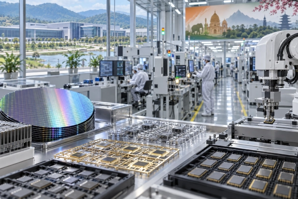
Tata Electronics has signed a Memorandum of Understanding with Japan’s Enomoto Co. Ltd. to strengthen the semiconductor packaging ecosystem around its upcoming high-volume assembly and test facility at Jagiroad in Assam. The agreement brings Enomoto’s expertise in precision semiconductor components, tooling and advanced manufacturing into one of India’s largest semiconductor packaging projects and is intended to support the development of a more complete domestic supply chain for chip assembly and testing.
Announced on 18 September 2026, the partnership will focus on improving technology readiness at Jagiroad while exploring the localisation of critical semiconductor components in India. Tata Electronics and Enomoto will also examine opportunities for engineering collaboration, technology transfer and capability development, giving the relationship a broader scope than a conventional supplier agreement.
The collaboration is particularly important because semiconductor packaging depends on a network of specialised precision components and materials that are often imported. By exploring local production and engineering support, the two companies are attempting to reduce this dependence while strengthening the industrial ecosystem around Tata Electronics’ Assam facility.
Enomoto to Support Jagiroad Packaging Operations
Under the agreement, Enomoto will bring its research and development capabilities, manufacturing expertise and precision-component technologies to support Tata Electronics’ semiconductor packaging operations at Jagiroad. The collaboration is intended to accelerate readiness for high-volume assembly and test while also helping Tata Electronics build greater domestic capability in components required for packaging.
Semiconductor packaging is the stage at which fabricated silicon dies are electrically connected, protected and assembled into forms that can be incorporated into electronic systems. The process has a direct impact on reliability, thermal management, electrical performance and long-term durability, making packaging an increasingly important part of semiconductor engineering rather than simply a final protective step.
As chips become more complex, packaging technologies are also becoming more advanced. Modern architectures increasingly combine multiple dies, memory devices, sensors and other functions within a single package, placing greater demands on precision components, substrates, interconnects and manufacturing equipment.
Localisation of Lead Frames Under Exploration
One of the most significant elements of the Tata Electronics–Enomoto agreement is the proposed exploration of lead-frame manufacturing in India. Lead frames are precision metal structures used in many semiconductor packages to provide both mechanical support for the silicon die and an electrical connection between the chip and the external circuitry.
Although they appear relatively simple compared with the semiconductor die itself, lead frames require precise stamping, forming, plating and dimensional control. Small variations in their geometry or surface quality can affect wire bonding, package reliability and electrical performance, making them an important part of the semiconductor packaging supply chain.
Localising lead-frame production would therefore strengthen an upstream layer of India’s semiconductor ecosystem that currently depends heavily on imports. It could also create opportunities for Indian precision-engineering companies to participate in a specialised manufacturing segment that supports not only Tata Electronics but potentially other semiconductor packaging facilities in the future.
Enomoto Brings Precision Manufacturing Expertise
Enomoto is an established Japanese manufacturer with decades of experience in semiconductor lead frames, precision electronic components, tooling and automated manufacturing systems. Its capabilities include high-precision stamping, die engineering and fine metal and plastic processing for semiconductor, automotive, optoelectronic and industrial applications.
This expertise is relevant to Tata Electronics because high-volume semiconductor packaging requires components manufactured to extremely tight tolerances. Packaging lines operate at high speed and demand consistent dimensional accuracy across millions of components, leaving little room for manufacturing variation.
By working with Enomoto, Tata Electronics gains access to a company with experience in the specialised component technologies needed to support reliable semiconductor packaging. The partnership also creates a potential pathway for transferring manufacturing knowledge and process expertise into India as the Jagiroad facility scales up.
Technology Transfer and Engineering Cooperation
The MoU also provides for the exploration of technology transfer and engineering collaboration between the two companies. This could allow Tata Electronics to move beyond the import of finished components and develop greater domestic capability in the design, manufacture and qualification of packaging-related parts.
Such cooperation is important because semiconductor packaging requirements vary according to chip architecture, voltage, power density, heat generation and end application. Components used in automotive electronics, for example, may need to meet very different reliability standards from those used in consumer or communications equipment.
Developing local engineering capability would allow Indian manufacturers to adapt packaging components more quickly to specific customer requirements. It could also reduce lead times and improve coordination between component suppliers and Tata Electronics’ assembly and test operations.
Jagiroad Emerging as a Major Semiconductor Packaging Hub
Tata Electronics is investing more than US$3 billion in its semiconductor assembly and test facility at Jagiroad in Assam. The plant is being developed on a large industrial site near Guwahati and is intended to become one of India’s largest semiconductor packaging facilities.
The project is expected to support a range of packaging technologies, including conventional wire-bond packages, flip-chip packaging and more advanced integrated system packaging. These capabilities will allow Tata Electronics to serve customers across automotive electronics, communications, computing, industrial systems and artificial intelligence.
The scale of the Jagiroad project means that the facility will require a substantial supplier ecosystem covering lead frames, substrates, bonding materials, moulding compounds, precision tooling, testing systems and other specialised inputs. The Enomoto partnership directly addresses one of these supporting industrial layers.
Advanced Packaging Is Becoming More Important
Semiconductor performance is increasingly influenced by packaging as much as by the chip itself. As transistor scaling becomes more difficult and expensive, semiconductor companies are using advanced packaging to improve system performance by combining multiple dies and functions within compact architectures.
Technologies such as flip-chip, system-in-package and other advanced packaging methods can shorten electrical connections, improve thermal performance and allow processors, memory, sensors and power-management devices to be integrated more efficiently.
This trend has made packaging a strategic technology area in its own right. Countries seeking to build semiconductor capability can no longer focus only on wafer fabrication because packaging and testing increasingly determine how chips are integrated into real-world systems.
Tata Electronics’ investment in Jagiroad is therefore important not merely as an assembly project but as part of India’s attempt to build capability in a segment of the semiconductor value chain that is becoming more technologically sophisticated.
Building a Domestic Packaging Component Ecosystem
A large semiconductor packaging plant cannot operate efficiently without a dependable network of suppliers. In addition to lead frames, packaging requires substrates, bonding wire, moulding materials, adhesives, precision tooling, chemicals, inspection systems and automated handling equipment.
If most of these components continue to be imported, India’s packaging operations would remain dependent on overseas supply chains even after local assembly capacity is established. The Enomoto partnership seeks to address this problem by examining which components and manufacturing processes can be localised around the Jagiroad operation.
Developing these capabilities domestically could shorten lead times and reduce exposure to international logistics disruptions. It could also help build a more resilient semiconductor ecosystem by allowing suppliers and packaging companies to coordinate more closely.
India-Japan Semiconductor Cooperation Deepens
The Tata Electronics–Enomoto agreement also reflects the growing role of Japanese companies in India’s semiconductor expansion. Japan has long-standing strengths in semiconductor materials, chemicals, precision components, equipment and advanced manufacturing, making it a natural partner for India as the country builds new semiconductor infrastructure.
India, in turn, offers a rapidly expanding electronics market, a large engineering workforce and growing government support for semiconductor manufacturing. These complementary strengths have created a steady increase in partnerships between Indian companies and Japanese technology suppliers.
Enomoto’s participation adds precision packaging components to this broader pattern of cooperation. It follows other India-Japan semiconductor partnerships involving materials, chemicals, logistics and manufacturing technologies.
Tata Electronics Builds a Wider Network Around Jagiroad
The Enomoto agreement is one of several partnerships Tata Electronics is developing around its Assam packaging facility. The company is working with international technology and equipment suppliers to strengthen advanced packaging capabilities, improve manufacturing readiness and build a more diversified customer base.
Tata Electronics has also partnered with Besi, a major semiconductor assembly-equipment company, to support advanced packaging technology at Jagiroad. That relationship is intended to improve access to specialised packaging equipment, training and process know-how as Tata Electronics prepares for high-volume operations.
The company has separately announced cooperation with Nexperia covering semiconductor manufacturing, technology and innovation. Under that partnership, Nexperia products are expected to make use of Tata Electronics’ packaging and test capabilities in India.
Together, these agreements indicate that Tata Electronics is building a broader industrial ecosystem rather than treating Jagiroad as a standalone manufacturing plant.
Jagiroad Could Develop Into a Semiconductor Cluster
The presence of a large anchor facility can encourage supporting companies to establish operations nearby. Semiconductor packaging creates demand for materials, precision components, equipment servicing, tooling, testing, logistics and specialised engineering support, giving suppliers a reason to locate close to the main manufacturing centre.
If Tata Electronics succeeds in attracting component manufacturers and technology partners to Assam, Jagiroad could gradually develop into a broader semiconductor cluster. Such clustering is common in mature semiconductor regions because it reduces logistics costs, shortens response times and improves collaboration between manufacturers and suppliers.
The Enomoto agreement is relevant in this context because localisation of components such as lead frames could become one of the first steps towards developing a supplier network around the Assam facility.
Expanding Advanced Manufacturing Into Northeast India
The Jagiroad project is also significant because of its location in northeastern India. Much of the country’s electronics and semiconductor activity has historically been concentrated in regions such as Karnataka, Tamil Nadu, Telangana, Gujarat and the National Capital Region.
The Assam facility extends semiconductor manufacturing into a part of India that has not previously hosted industry at this technological scale. Tata Electronics has indicated that the project will generate substantial direct and indirect employment while also creating opportunities for suppliers, logistics providers and technical-service companies.
If supporting industries begin to develop around the plant, the impact could extend beyond semiconductor packaging itself by creating a new advanced-manufacturing base in the region.
From Assembly Plant to Semiconductor Ecosystem
India’s semiconductor strategy is increasingly moving beyond individual manufacturing projects towards the creation of complete ecosystems. A functioning semiconductor industry requires chip design, fabrication, packaging, testing, materials, precision components, equipment suppliers, logistics and skilled manpower to operate together.
The Enomoto partnership addresses the precision-component and manufacturing-technology part of this value chain. By exploring local lead-frame production, engineering cooperation and technology transfer, the collaboration could help reduce dependence on imported packaging inputs while building a specialised manufacturing base within India.
For Tata Electronics, the agreement strengthens the industrial foundation of the Jagiroad facility. For India, it represents another step towards creating a semiconductor ecosystem that includes not only large manufacturing plants but also the specialised suppliers needed to keep those plants operating at scale.
A Building Block for India’s Advanced Packaging Ambitions
The Tata Electronics–Enomoto partnership may appear less dramatic than the announcement of a new semiconductor fab, but such supplier relationships are essential to building a sustainable semiconductor industry. Packaging operations depend on a reliable flow of precision components, materials and technical expertise, and these supporting capabilities must develop alongside the main manufacturing facilities.
Enomoto brings decades of experience in semiconductor components and precision manufacturing, while Tata Electronics provides the scale of a major new packaging operation in Assam. If the localisation plans move forward, the partnership could help turn Jagiroad from a large assembly and test facility into the nucleus of a broader semiconductor packaging and component ecosystem.
References
- Tata Electronics — Tata Electronics and Enomoto Sign Memorandum of Understanding to Strengthen Semiconductor Packaging Ecosystem in India, 18 September 2026
https://www.tataelectronics.com/w/tata-electronics%E2%80%AFand%E2%80%AFenomoto-sign-memorandum-of-understanding-to-strengthen-semiconductor-packaging-ecosystem-in-india - Tata Electronics — Semiconductor Assembly and Test: Jagiroad, Assam Facility
https://www.tataelectronics.com/semiconductor-assembly-and-test - Tata Electronics — Tata Electronics and Besi Enter Strategic Partnership to Strengthen Advanced Packaging Capabilities, 17 September 2026
https://www.tataelectronics.com/w/tata-electronics-and-besi-enter-strategic-partnership-to-strengthen-advanced-packaging-capabilities - Tata Electronics — Nexperia and Tata Electronics Announce Strategic Partnership Across Semiconductor Manufacturing, Technology and Innovation, 17 September 2026
https://www.tataelectronics.com/w/nexperia-and-tata-electronics-announce-strategic-partnership-across-semiconductor-manufacturing-technology-and-innovation
You may also like
-
India to Establish First Precision Manufacturing Institute Under Semicon 2.0
-
India-Made Semiconductor Products Begin Reaching Global Markets as Domestic Ecosystem Expands
-
Semicon 2.0 Targets 200 Chip-Design Companies and One Lakh Semiconductor Technicians
-
LightSpeed Photonics Plans India Packaging Pilot Line, Targets 50% Local Production by 2028
-
Tata Electronics, Sojitz and NRS Build Critical Materials Supply Chain for ₹91,000-Crore Dholera Semiconductor Fab
