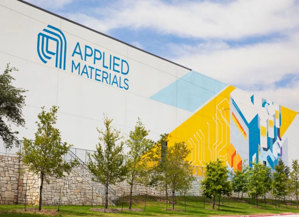
US semiconductor equipment major Applied Materials has announced plans to invest $5 billion in India over the next decade, marking a significant expansion of its research, engineering and supply-chain presence as the country attempts to build a semiconductor industry extending well beyond chip assembly and packaging.
The investment was announced at SEMICON India 2026 in New Delhi on September 17. Applied Materials said its plans would concentrate on semiconductor research and development, expansion of its Indian supply chain and growth of its workforce in the country.
The announcement is particularly significant because Applied Materials operates much deeper in the semiconductor manufacturing chain than consumer electronics or conventional chip-design companies. The company develops equipment, materials-engineering technologies and manufacturing systems used by semiconductor producers to fabricate increasingly advanced chips. Its decision to expand research and supply-chain activity in India therefore connects the country with the industrial infrastructure behind semiconductor manufacturing itself.
India to Take a Larger Role in Applied Materials’ Global R&D
India is already an important engineering and research base for Applied Materials. The company has operated in the country for more than two decades, with Indian teams working across research and development, product and software engineering, design, validation and product lifecycle development.
Applied Materials describes India as a strategic innovation centre within its global network rather than simply an overseas engineering location. Its existing infrastructure includes laboratories, engineering facilities and the India Validation Center in Bengaluru, which the company describes as India’s first 300-mm semiconductor R&D facility of its kind.
The new investment will expand this foundation considerably. Instead of entering India from scratch, Applied Materials is increasing the scale of an engineering ecosystem that is already connected with its global semiconductor equipment business.
This distinction matters for India’s semiconductor ambitions. Building fabrication plants is only one part of creating a sustainable chip industry. Fabs depend on highly specialised equipment, materials, process technologies, engineering expertise and validation capabilities. Developing some of these activities in India would broaden the country’s participation in the semiconductor value chain beyond the manufacturing plants currently under construction.
Indian Supply Chain Set for Major Expansion
A substantial part of the $5 billion programme will be directed towards expanding Applied Materials’ Indian supply chain. Reports accompanying the announcement indicate that the company intends to increase its India-based supply-chain capacity substantially by 2035.
Semiconductor manufacturing equipment is extraordinarily complex. A single production system can contain precision-engineered mechanical components, vacuum equipment, electronics, power systems, advanced materials, sensors and other specialised parts that must meet demanding tolerances and reliability requirements.
Expanding sourcing in India could therefore create opportunities for domestic precision-engineering, electronics and advanced-manufacturing companies capable of entering Applied Materials’ supplier network. The value of such participation would extend beyond supplying the Indian semiconductor market because components meeting the company’s standards could potentially become part of a global manufacturing chain.
This is one of the areas where India’s semiconductor strategy is beginning to move beyond individual fabrication projects. A sustainable industry requires equipment suppliers, materials companies, component manufacturers, testing facilities, engineering services and skilled workers around the fabs themselves.
Applied Materials’ decision to expand its supplier ecosystem gives Indian manufacturers an opportunity to enter that supporting industrial structure.
Advanced Research Park Planned in Bengaluru
The company’s plans also include a large advanced semiconductor research park in Bengaluru. Reports from SEMICON India indicate that the proposed facility will occupy approximately 140 acres and form an important part of Applied Materials’ expanded Indian research presence.
Bengaluru already hosts a substantial concentration of India’s semiconductor design and engineering workforce. Adding advanced equipment research and validation infrastructure would deepen the city’s role beyond chip design and software engineering.
For semiconductor equipment companies, research facilities are closely connected with the manufacturing process itself. New generations of chips require advances in deposition, materials modification, metrology, patterning and other highly specialised manufacturing technologies. As transistors and interconnects become smaller and increasingly three-dimensional, the equipment used to manufacture them must solve progressively more difficult engineering problems.
An expanded Applied Materials research presence would therefore place Indian engineers closer to the development of the technologies used inside semiconductor fabs rather than limiting their participation to downstream applications.
Workforce Expansion Forms Third Pillar of Investment
Applied Materials also plans to expand its Indian research and engineering workforce substantially during the investment period. The company’s Indian operations already contribute to global R&D and product engineering, and the new programme is expected to increase the number of engineers involved in those activities.
Workforce development has become an important part of India’s semiconductor strategy because fabs and equipment companies require specialised expertise that cannot be created merely by constructing manufacturing facilities. Semiconductor process engineering, materials science, equipment development and advanced manufacturing require experienced technical personnel and long-term collaboration between companies, universities and research institutions.
The presence of large international semiconductor companies can help create this capability by exposing Indian engineers to manufacturing technologies and global product-development programmes. Over time, employees and suppliers trained within these ecosystems can also contribute to domestic semiconductor companies and startups.
Applied Materials has already worked with Indian academic institutions and industry partners, giving the company an existing base for expanding this talent pipeline.
Investment Comes as India’s Semiconductor Programme Enters a New Phase
The announcement comes as India moves into the second phase of its semiconductor programme. Twelve semiconductor projects have been approved under government incentive programmes during the past five years, while commercial production has begun at three chip-packaging facilities.
The country is also attempting to broaden its policy beyond fabrication and packaging. Semicon 2.0 places greater emphasis on chip design, research and development, semiconductor equipment, materials, chemicals, gases, substrates and workforce development.
That broader approach is important because no major semiconductor manufacturing centre operates through fabs alone. A fabrication plant depends on a dense network of companies supplying equipment, chemicals, gases, wafers, components, software and specialised engineering services.
Applied Materials sits within precisely this part of the industry. Its expanded Indian presence therefore aligns with the effort to build more of the supporting semiconductor ecosystem inside the country.
India’s semiconductor consumption is projected by government estimates to reach around $110 billion by 2030, compared with roughly $45-50 billion in 2025. At the same time, global semiconductor companies are reassessing supply chains as demand from artificial intelligence, data centres, automotive electronics and advanced computing continues to grow.
India Competing for a Place in the Semiconductor Equipment Chain
The global semiconductor industry remains concentrated in a relatively small number of countries, and manufacturing equipment is one of its most technologically demanding segments. Companies supplying fabrication equipment possess decades of accumulated expertise in materials engineering, precision manufacturing and process control.
India is therefore unlikely to create a complete semiconductor equipment industry simply by attracting fabrication plants. The more immediate opportunity lies in bringing research, validation, engineering and parts of the global equipment supply chain into the country while domestic capabilities develop alongside them.
Applied Materials’ $5 billion programme fits this model. The investment combines research infrastructure with supplier development and workforce expansion rather than concentrating exclusively on one manufacturing facility.
That combination could also create opportunities for Indian precision manufacturers and engineering companies that currently operate outside the semiconductor industry. Qualifying as suppliers to semiconductor equipment companies requires stringent standards, but companies that successfully enter such supply chains gain exposure to a technologically demanding global market.
From Chip Assembly Towards a Broader Industrial Ecosystem
India’s first phase of semiconductor development concentrated heavily on attracting fabrication, assembly and packaging projects. The next stage will depend on whether the country can build the industrial structure surrounding those plants.
Equipment, materials, gases, chemicals, precision components, research facilities and engineering talent determine how deeply a country participates in semiconductor manufacturing. Without them, even domestic fabs remain heavily dependent on overseas supply chains.
Applied Materials’ investment does not eliminate that dependence, nor does it mean India is becoming self-sufficient in semiconductor equipment. What it does is bring a larger portion of one of the industry’s most sophisticated technology ecosystems into the country.
The scale of the planned investment, combined with the proposed research expansion and supplier development, makes the announcement more significant than another semiconductor manufacturing project. Applied Materials is placing India within its longer-term research and equipment supply-chain strategy at a time when the country’s first major semiconductor manufacturing investments are beginning to take shape.
For India, the opportunity now lies in using that presence to develop domestic engineering capability, qualify Indian companies for global semiconductor supply chains and gradually increase the amount of semiconductor technology and intellectual property created within the country.
REFERENCES
- Applied Materials — India Overview. Official company information on Applied Materials’ research, engineering and semiconductor technology operations in India.
https://www.appliedmaterials.com/in/en/about/india-overview.html - Applied Materials — SEMICON India 2026. Official company event page detailing Applied Materials’ participation and India’s role in its global semiconductor strategy.
https://www.appliedmaterials.com/in/en/news-and-media/events/semicon-india-2026.html - Reuters, “Applied Materials to invest $5 billion in India as Modi’s flagship chip event kicks off,” published 17 September 2026.
https://www.reuters.com/world/asia-pacific/applied-materials-invest-5-billion-india-modis-flagship-chip-event-kicks-off-2026-09-17/ - Business Standard, “Applied Materials to invest $5 billion in India over next decade,” published 17 September 2026.
https://www.business-standard.com/companies/news/applied-materials-to-invest-5-billion-in-india-over-next-decade-126091700558_1.html - YourStory, “Applied Materials commits $5B to India semiconductor push,” published 17 September 2026.
https://yourstory.com/2026/09/applied-materials-commits-usd-5b-to-india-semiconductor-push
You may also like
-
India and Bhutan Complete Two-Way UPI Connectivity, Enabling Digital Payments for Travellers in Both Countries
-
India Launches $13.5 Billion Semiconductor Mission 2.0 as Domestic Chips Begin Reaching Customers
-
HAL to Hand Over Tejas Twin-Seat Fighters and HTT-40 Trainers to IAF, Dhruv NG Helicopters to Pawan Hans
-
Nearly 70% of Valmo Delivery Partners Filing ITRs Are First-Time Tax Filers, ₹2 Crore in Refunds Claimed
-
Southern Railway Achieves 100% Electrification of Entire 5,068-km Broad-Gauge Network
