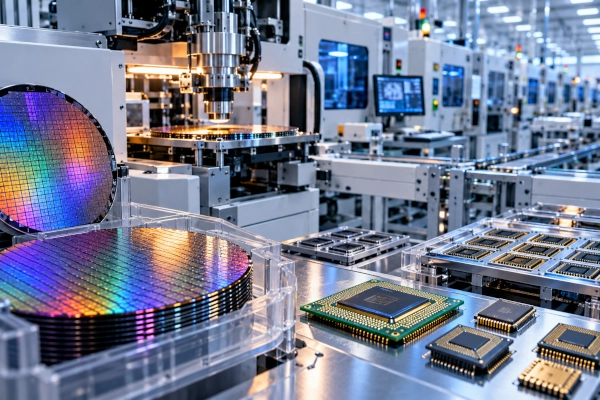
Indian semiconductor and electronics companies have proposed substantial new investments in Madhya Pradesh, strengthening the state’s efforts to emerge as a centre for advanced electronics manufacturing, chip design and technology development. The proposals were announced during the Madhya Pradesh Semiconductor Summit 2026, held in Indore on 23 and 24 October.
According to investment details reported on 25 October 2026, the state attracted proposals valued at more than ₹15,425 crore across semiconductor-related industries, electronics manufacturing, data centres and other high-technology sectors. The projects collectively carry projections of more than 14,450 employment opportunities.
The summit brought together semiconductor companies, electronics manufacturers, technology entrepreneurs, research organisations and international representatives. Companies including Una Ecosystems, Spintronics AI Semiconductors, Lalwala Industries, Indusilica Semiconductors and Truechip Solutions presented plans to develop manufacturing, design and engineering capabilities in Madhya Pradesh.
The announcements reflect growing interest in expanding India’s semiconductor ecosystem beyond wafer fabrication to encompass chip design, packaging, testing, electronic systems and specialised engineering services. However, the announced figures represent proposed investments, land-allotment initiatives and anticipated employment rather than completed projects.
Madhya Pradesh Semiconductor Summit Attracts Major Industrial Interest
The two-day semiconductor summit was organised at the Brilliant Convention Centre in Indore as part of Madhya Pradesh’s efforts to attract investment in emerging technologies and advanced manufacturing.
Chief Minister Mohan Yadav inaugurated the event and held individual meetings with representatives of more than 12 companies and institutions interested in establishing or expanding operations in the state.
During the opening day, the government reported fresh investment proposals exceeding ₹5,800 crore, with the potential to generate more than 10,000 employment opportunities. The proposals covered semiconductor design, electronics system design and manufacturing, healthcare technology, digital infrastructure and related industries.
Separately, the state issued letters of intent for land allotment to five companies planning projects valued at approximately ₹9,625 crore. These projects were associated with projections of more than 4,450 direct jobs across Bhopal, Indore and Gwalior.
The two categories of announcements reflect different stages of industrial development. Investment proposals indicate a company’s expressed interest, while letters of intent for land allotment represent progress towards identifying locations for proposed projects. Neither establishes that the full investment has been deployed or that manufacturing operations have commenced.
The summit also attracted more than 1,000 participants, including representatives from Japan, South Korea, Taiwan and Sweden. Discussions focused on semiconductor technology, artificial intelligence, electronics manufacturing, advanced packaging, photonics and quantum technologies.
Una Ecosystems Proposes ₹2,000 Crore Electronics Manufacturing Investment
Una Ecosystems emerged among the prominent companies participating in the summit, presenting a proposal involving an investment of approximately ₹2,000 crore.
The company discussed establishing an electronics system design and manufacturing facility in Madhya Pradesh, with an estimated employment potential of 2,000 positions.
Electronics system design and manufacturing, commonly abbreviated as ESDM, encompasses activities ranging from electronic circuit design and component integration to product assembly, testing and manufacturing.
Such facilities support the production of electronic systems used in telecommunications, consumer appliances, industrial equipment, automotive applications and other sectors.
The summit also featured a land-allotment proposal associated with Una Ecosystems for a lithium-cell manufacturing facility at Electronics Manufacturing Cluster-2 in Bhopal. Reports identified a proposed capacity of 1.5 gigawatt-hours and an investment of ₹2,000 crore.
The proposed battery manufacturing facility is relevant to India’s expanding energy storage industry, particularly as electric vehicles and renewable energy systems increase demand for domestically manufactured lithium-ion cells.
The available reports do not fully clarify whether the ESDM announcement and the lithium-cell land-allotment proposal represent separate investment commitments or different descriptions of the same ₹2,000 crore project. They should therefore not be added together as independently confirmed investments.
The company’s participation illustrates how state-level technology initiatives are attracting interest from businesses operating across interconnected electronics and energy-storage industries.
Spintronics AI Semiconductors Plans ₹1,800 Crore Investment in Two Phases
Spintronics AI Semiconductors proposed an investment of approximately ₹1,800 crore in Madhya Pradesh, with the planned expenditure expected to take place in two phases.
The Hyderabad-based company also participated in discussions concerning semiconductor design, product development and engineering support activities.
Semiconductor design represents an important part of the chip manufacturing value chain. It involves developing the circuit architectures, functional components and physical layouts that determine how semiconductor devices operate.
Chip design companies may develop integrated circuits for applications involving computing, communications, sensing, industrial automation and specialised electronic systems.
Such activities require engineering capabilities in digital and analogue circuit design, verification, simulation, testing and related software tools.
The company’s proposed investment adds to interest in establishing semiconductor engineering activities in Madhya Pradesh. Its participation also reflects the increasing importance of connecting chip design expertise with manufacturing, packaging and testing capabilities.
Land identification for Spintronics was reportedly under consideration following the summit, indicating that its industrial plans remained at a preparatory stage.
The eventual scope of the investment will depend on project implementation, infrastructure availability, technical requirements and subsequent company decisions.
Lalwala Industries Proposes ₹1,200 Crore for Semiconductor Manufacturing and Chip Design
Lalwala Industries presented an investment proposal valued at approximately ₹1,200 crore for semiconductor manufacturing and chip design activities.
The announcement formed part of the company’s discussions with Madhya Pradesh officials during the Indore summit.
The proposal is relevant to India’s efforts to strengthen domestic semiconductor capabilities across several stages of electronic product development.
Semiconductor manufacturing and design encompass different technological activities. Chip design involves the development and verification of integrated circuits, while semiconductor manufacturing can include wafer fabrication, packaging, assembly, testing or other production processes.
The available summit reporting does not establish the precise manufacturing processes Lalwala Industries intends to undertake. It would therefore be premature to describe the proposed facility as a full semiconductor wafer fabrication plant.
Nevertheless, the scale of the announced proposal indicates interest in establishing a substantial industrial presence within Madhya Pradesh’s emerging technology ecosystem.
The project could create opportunities for specialised engineering services, technical employment and industrial cooperation as further details of its proposed operations become available.
Indusilica Semiconductors and Truechip Solutions Expand Chip Design Interest
Alongside the larger investment proposals, several specialised semiconductor businesses expressed interest in smaller technology-focused projects.
Indusilica Semiconductors proposed an investment of approximately ₹100 crore, with an estimated employment potential of 150 positions.
The company’s representatives discussed opportunities for establishing operations in Madhya Pradesh and participating in the state’s growing semiconductor ecosystem.
Truechip Solutions presented an investment proposal of approximately ₹10 crore, with projections of 50 jobs associated with the proposal.
Truechip operates in semiconductor design-related engineering services, an area that supports the development and verification of complex integrated circuits.
Verification is an essential part of semiconductor design because engineers must establish whether a circuit performs its intended functions before proceeding to costly manufacturing stages.
Design-verification activities may involve simulation, test environments, hardware description languages and specialised electronic design automation tools.
The participation of companies such as Indusilica and Truechip demonstrates the importance of specialised engineering capabilities alongside large industrial investments.
A competitive semiconductor ecosystem requires design companies, engineering service providers, manufacturing facilities, testing organisations and trained professionals working across different stages of the value chain.
Nanodrites Technology Proposes ₹65 Crore Investment
Nanodrites Technology was another company identified among the investment proposals presented during the summit.
The company proposed an investment of approximately ₹65 crore, with an estimated employment potential of 140 positions.
Its participation formed part of wider discussions involving advanced technology enterprises interested in Madhya Pradesh’s emerging industrial infrastructure.
Smaller technology companies can play an important role in developing specialised capabilities within semiconductor and electronics ecosystems.
Their activities may include engineering services, product development, specialised design, software tools and technical support for larger industrial manufacturers.
The summit reporting does not provide sufficient detail to establish the precise products, manufacturing processes or technological capabilities planned under Nanodrites Technology’s proposal.
The investment should therefore be understood as an announced project proposal rather than evidence of a specific semiconductor production capability already established.
Its inclusion alongside larger projects demonstrates the state’s intention to attract businesses of different sizes and technical specialisations.
Kaynes Electronics and Meena Circuits Plan New Manufacturing Facilities
The summit also highlighted proposed electronics manufacturing investments involving Kaynes Electronics and Meena Circuits.
Kaynes Electronics received a land-allotment letter of intent associated with a proposed investment of approximately ₹310 crore for an electronics manufacturing facility at Badwai IT Park in Bhopal.
The project was linked to an estimated employment potential of approximately 950 positions.
Meena Circuits presented plans for an electronics system design and manufacturing unit involving approximately ₹400 crore.
These proposed facilities would contribute to activities associated with electronic products, components and manufacturing services.
Electronics manufacturing is an important supporting industry for semiconductor development because completed semiconductor devices must be integrated into functional electronic products.
Printed circuit boards, electronic modules, industrial controllers and specialised assemblies all depend on a reliable network of component suppliers and manufacturing service providers.
The presence of electronics manufacturing companies can therefore complement investments in semiconductor design, assembly, packaging and testing.
The proposed projects also demonstrate the importance of connecting semiconductor policy with the wider industrial requirements of electronics manufacturing.
Gwalior Attracts ₹6,415 Crore Hyperscale Data Centre Proposal
One of the largest individual projects associated with the summit involved a proposed hyperscale data centre in Gwalior.
Cytech RE received a land-allotment letter of intent for a project involving an estimated investment of ₹6,415 crore at Ganga Malanpur.
The proposed facility would have a capacity of approximately 50 megawatts, according to the investment details announced during the summit.
Hyperscale data centres provide infrastructure for large-scale computing, cloud services, digital platforms and data processing.
They typically require substantial investments in electrical infrastructure, cooling systems, high-capacity network connections, physical security and computing equipment.
The growing demand for cloud computing and artificial intelligence has increased attention on data-centre development across India.
Although a data centre is not a semiconductor manufacturing facility, the industry depends heavily on advanced processors, memory devices, communications equipment and other electronic components.
The inclusion of data-centre investments in Madhya Pradesh’s broader technology programme illustrates the state’s ambition to attract complementary industries involved in digital infrastructure and advanced computing.
Indore Plans New Global Capability Centre and Engineering Facilities
Madhya Pradesh also announced proposed investments intended to strengthen its engineering services and technology workforce.
Auriga IT Solutions received a land-allotment letter of intent associated with a proposed ₹500 crore Global Capability Centre at Sinhasa IT Park in Indore.
The project carries an estimated employment potential of 3,500 positions.
Global Capability Centres perform specialised business and technical functions for organisations, including software development, research, engineering, analytics and other professional services.
The summit also included letters of intent for office space at the Electronics Complex in Pardesipura, Indore.
Seven companies received office-space allotment letters, with their proposed operations associated with approximately 1,280 employment opportunities.
The participating businesses included companies working in semiconductor design, electronic engineering, product development, information technology and emerging digital applications.
These developments reflect the role of technical services and research activities in supporting a broader semiconductor and electronics manufacturing ecosystem.
The availability of trained engineers, development facilities and specialised service companies can influence the attractiveness of an industrial region for manufacturing investments.
Semiconductor Design and Manufacturing Require Different Capabilities
India’s semiconductor development strategy involves several technologically distinct activities.
Chip design begins with the architecture and engineering of integrated circuits. Designers determine how electronic components will perform functions such as processing information, storing data, handling communications or controlling other devices.
Semiconductor wafer fabrication converts these designs into physical circuits through highly specialised manufacturing processes.
After fabrication, semiconductor dies undergo assembly, packaging and testing to produce components suitable for integration into electronic systems.
Electronics manufacturing then combines semiconductor devices with circuit boards, connectors, sensors and other components to create functional products.
Each stage requires different equipment, technical skills, industrial facilities and investment levels.
The Madhya Pradesh proposals cover several parts of this wider ecosystem, including chip design, electronics manufacturing and related technology infrastructure.
This diversity is significant because building a semiconductor industry involves more than attracting one large factory. The development of domestic capabilities requires cooperation among design businesses, manufacturers, suppliers, research institutions and engineering service providers.
The summit’s focus on several complementary industries reflects this broader understanding of semiconductor development.
Madhya Pradesh Plans Centres of Excellence in Semiconductors and Quantum Technologies
Chief Minister Mohan Yadav announced plans to establish a Semiconductor Centre of Excellence and a Centre of Excellence for Photonics and Quantum Technologies.
These initiatives are intended to support research, technological development, innovation and specialised workforce training.
Semiconductor engineering requires professionals with expertise in electronic circuit design, materials science, embedded systems, manufacturing processes, testing and quality assurance.
Advanced manufacturing operations also need technicians trained in equipment maintenance, industrial automation, process control and cleanroom operations.
Centres of Excellence can help connect academic institutions with industry requirements by supporting training programmes, research collaboration and access to specialised technical facilities.
Photonics and quantum technologies are emerging areas involving applications such as optical sensing, communications, advanced measurement systems and computing research.
The proposed institutions could help Madhya Pradesh develop technical capabilities extending beyond conventional electronics assembly.
Their effectiveness will depend on implementation, research infrastructure, industry participation and the availability of qualified scientific and engineering personnel.
Partnerships with National and International Technology Institutions
The Madhya Pradesh State Electronics Development Corporation exchanged memoranda of understanding with five institutions during the summit.
The participating organisations included the Electronics Sector Skills Council of India, SEMI India, Semiconductor Laboratory in Mohali, the International Semiconductor Industry Group in London and the Indian Institute of Creative Technologies in Mumbai.
The agreements aim to support semiconductor ecosystem development through industry collaboration, technical training, research, investment facilitation and the exchange of expertise.
Semiconductor Laboratory, Mohali, occupies an important position within India’s domestic semiconductor research and manufacturing infrastructure.
Its participation provides opportunities for institutional engagement involving semiconductor processes, technical knowledge and specialised training.
SEMI India represents a connection with the wider semiconductor industry ecosystem, including businesses and organisations involved in semiconductor manufacturing and related supply chains.
The summit also featured international participation from Japan, South Korea, Taiwan and Sweden.
These engagements reflect the importance of international cooperation in a semiconductor industry characterised by specialised equipment, globally distributed manufacturing processes and complex supply chains.
The memoranda establish frameworks for cooperation, while specific activities and outcomes will depend on subsequent implementation.
Madhya Pradesh Semiconductor Policy 2025 Offers Investment Incentives
The state government introduced the Madhya Pradesh Semiconductor Policy 2025 to support investment in chip design, semiconductor manufacturing and related industries.
Under the policy, eligible projects can receive support linked to capital expenditure or incentives available under central government semiconductor programmes.
The reported provisions include incentives equivalent to 25% of eligible capital expenditure or 50% of central government incentives, whichever is lower.
Eligible fabless semiconductor and intellectual property companies may receive support for development expenditure, subject to specified limits and conditions.
Other provisions include assistance involving stamp duty, registration expenses, interest costs and electricity tariffs.
The policy aims to address some of the challenges associated with establishing capital-intensive technology facilities.
Semiconductor and electronics manufacturers require reliable electricity supplies, specialised industrial infrastructure, efficient logistics and access to skilled technical workers.
A supportive policy framework can help attract companies, but long-term industrial growth also depends on successful project execution, commercial demand and the development of supporting supply chains.
The state’s ability to provide suitable infrastructure and maintain policy continuity will therefore be important as the proposed projects move towards implementation.
Indore-Ujjain Economic Corridor Identified for Advanced Technology Development
Madhya Pradesh has identified the Indore-Ujjain Economic Corridor as a priority location for semiconductor, electronics manufacturing and advanced packaging industries.
The region offers access to an established industrial base, educational institutions and commercial infrastructure.
Indore has developed capabilities in information technology, engineering services, education and industrial production, while surrounding industrial areas provide opportunities for manufacturing expansion.
The government’s plans aim to attract companies working across semiconductor design, electronic systems and specialised manufacturing processes.
A concentration of related businesses within a single region can create opportunities for cooperation among component suppliers, manufacturing companies, research institutions and technical service providers.
Industrial clusters can also support workforce development by creating sustained demand for specialised skills.
Madhya Pradesh’s emerging semiconductor plans seek to build these connections while encouraging investment in supporting industries such as digital infrastructure and advanced engineering.
The success of the proposed corridor will depend on the transition from investment proposals to operational projects and the establishment of reliable industrial capabilities.
New Investment Proposals Strengthen India’s Semiconductor Development Efforts
The investment proposals presented during the Madhya Pradesh Semiconductor Summit 2026 reflect growing interest among Indian companies in advanced electronics, semiconductor design and technology-driven manufacturing.
Una Ecosystems, Spintronics AI Semiconductors, Lalwala Industries, Indusilica Semiconductors, Truechip Solutions and other participating businesses represent different segments of the wider technology ecosystem.
Their proposed investments are complemented by plans involving electronics manufacturing facilities, data centres, engineering services and specialised training institutions.
Together, the announcements indicate an effort to build a broader industrial foundation capable of supporting semiconductor-related development in central India.
The projects remain at different stages, ranging from preliminary investment proposals to land-allotment letters and institutional cooperation agreements. Their eventual contribution will depend on implementation, commercial viability and the development of suitable infrastructure.
As India expands its semiconductor and electronics manufacturing capabilities, the participation of domestic technology enterprises can strengthen the industry’s technical depth and create opportunities for skilled employment.
Madhya Pradesh’s focus on manufacturing, chip design, research and industrial infrastructure adds another regional dimension to India’s efforts to develop a competitive semiconductor ecosystem and increase technological self-reliance.
References
- Madhya Pradesh Government, 23 October 2026. Official announcements concerning the inauguration of Madhya Pradesh Semiconductor Summit 2026, investment proposals, employment projections and institutional cooperation agreements.
- Business Standard, 25 October 2026. MP Semicon Summit Draws ₹15,425 Crore Investment Proposals, 14,000 Jobs in Sight. Detailed reporting on the summit’s investment proposals, participating companies and land-allotment developments.
- Business Standard, 23 October 2026. Madhya Pradesh Gets ₹5,800 Crore in Semiconductor Investment Proposals. Company-specific details involving Una Ecosystems, Spintronics AI Semiconductors, Lalwala Industries and other technology enterprises.
- The Indian Express, 24 October 2026. From Data Centres to Lithium Cells, Madhya Pradesh Courts ₹9,625 Crore in Tech Investments. Information concerning proposed facilities involving Cytech RE, Una Ecosystems, Kaynes Electronics, Meena Circuits and Auriga IT Solutions.
- The Times of India, 23 October 2026. MP’s ₹5,800-Crore Investment Push to Generate Over 10,000 Jobs. Coverage of the summit, industry participation and proposed employment opportunities.
- Madhya Pradesh Semiconductor Policy 2025. Government policy framework detailing incentives and support mechanisms for semiconductor manufacturing, fabless design and related industries.
- Ministry of Electronics and Information Technology, Government of India. India Semiconductor Mission. National policy framework concerning semiconductor manufacturing, assembly, testing, packaging and chip design.
You may also like
-
CSIR-CRRI Partners with Industry to Develop Advanced Indigenous Airport Runway and Pavement Materials
-
Paras Semiconductors Secures 43 Acres in Madhya Pradesh for Proposed ₹6,200 Crore Advanced Chip Packaging Facility
-
Petronet LNG Plans ₹1,200 Crore Joint Venture for Ten Compressed Biogas Plants Across India
-
India Seeks South Korean Shipbuilding Partnerships as Sarbananda Sonowal Begins Four-Day Visit to Busan
-
Koraput Kalajeera Rice of Odisha: The GI-Tagged Aromatic Heritage of India’s Ancient Rice-Growing Region
