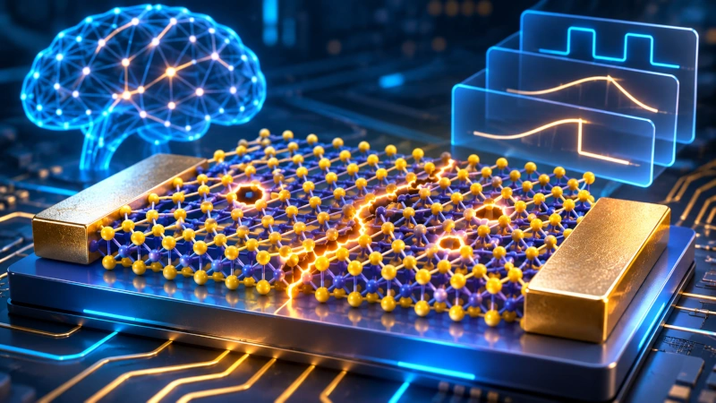
Researchers at the Indian Institute of Technology (IIT) Mandi have demonstrated how microscopic structural defects in an ultrathin semiconductor material can be utilised to develop advanced electronic memory devices with multiple switching capabilities. The research, reported on November 17–18, 2026, explores the use of tungsten disulphide (WS₂), a two-dimensional material, to create electronic components that could contribute to the development of next-generation memory systems and brain-inspired computing technologies.
The study demonstrates that imperfections traditionally regarded as undesirable during semiconductor manufacturing can be used to control electrical behaviour in specially designed devices. By examining the interaction between microscopic cracks and missing sulphur atoms in tungsten disulphide, the researchers identified mechanisms that enable a single electronic device to exhibit different forms of resistive switching.
The research was led by Professor Viswanath Balakrishnan of IIT Mandi, with contributions from Anjali Sharma, Yadu Chandran, Bhumit Luhar and collaborating researchers. Their findings were published in the international scientific journal Advanced Functional Materials in a paper titled Crack–Defect Landscapes Enable Multimodal Memristive Switching in WS₂ Mono-Bilayers.
The development is particularly significant because resistive switching devices, commonly known as memristors, are being investigated as potential components of future computing architectures that combine information storage and processing.
Turning Material Defects into Functional Electronic Features
Conventional semiconductor manufacturing generally seeks to minimise structural defects because imperfections can interfere with the predictable movement of electrical charges and reduce device reliability. However, the IIT Mandi study demonstrates that certain defects can be deliberately exploited to create useful electrical characteristics.
The researchers investigated tungsten disulphide, a semiconductor belonging to the family of transition metal dichalcogenides. These materials can be prepared in extremely thin layers, sometimes only one or two atomic layers thick, making them attractive candidates for research into miniaturised electronic devices.
During material synthesis, imperfections such as missing atoms, microscopic cracks and irregularities between crystalline regions may develop. In tungsten disulphide, the absence of sulphur atoms creates vacancies that can influence the distribution and movement of electrical charges.
The researchers found that microscopic cracks within the material can provide preferential pathways associated with the migration of vacancies and charged species. These interactions influence how the device conducts electricity when an external voltage is applied.
The central discovery is that the interaction between structural cracks and atomic vacancies can be used to produce different electrical memory behaviours within the same device architecture.
This finding provides a new perspective on defect engineering, an area of materials science concerned with controlling imperfections to obtain desired physical and electronic properties.
Understanding Memristors and Electronic Memory
A memristor is an electronic device whose resistance can change in response to an applied electrical stimulus and, under suitable conditions, retain information about its previous electrical state.
This property makes memristors attractive for research into non-volatile memory systems, where stored information can remain available even after the external power supply is removed.
In conventional computer architectures, processors perform calculations while separate memory components store information. Data must frequently move between these components, consuming time and electrical energy.
Memristive devices offer opportunities to investigate alternative computing architectures in which information storage and certain computational functions can occur within closely integrated hardware.
The electrical resistance of a memristor can represent stored information. By controlling changes in resistance, researchers can investigate devices capable of operating in different electrical states.
Some memristive devices exhibit abrupt changes between distinct resistance levels, while others can undergo gradual changes in conductance.
These characteristics are important because different forms of electrical switching can support different functions in emerging computing systems.
IIT Mandi Demonstrates Multiple Switching Mechanisms in a Single Device
The IIT Mandi researchers fabricated tungsten disulphide-based devices using chemical vapour deposition, a technique widely employed in semiconductor and advanced materials research.
Chemical vapour deposition allows thin material layers to form through controlled chemical reactions involving gaseous precursors. The resulting structures can be studied to understand how their composition, thickness and microscopic features influence electronic behaviour.
The research team examined devices containing different concentrations of sulphur vacancies and structural irregularities, including microscopic cracks.
Their experiments demonstrated that electrical switching could occur through more than one physical mechanism.
One mechanism involved vacancy redistribution along crack boundaries, contributing to filamentary resistive switching. Another involved charge trapping and changes in the Schottky barrier at the interface between tungsten disulphide and the metal contacts.
A Schottky barrier is an energy barrier that can form where a semiconductor meets a metal. Changes in this barrier can influence the movement of electrical charges and consequently alter the resistance of an electronic device.
The interaction between these mechanisms enabled the researchers to observe different switching characteristics within the same planar device.
The ability to obtain multiple electrical switching behaviours from one material system is important because future electronic architectures may require devices that perform several memory and information-processing functions.
The research provides experimental evidence connecting microscopic material structures with the electrical behaviour observed in these devices.
Devices Exhibit Analog and Digital Switching Characteristics
An important outcome of the research was the observation of different resistive switching behaviours, including gradual analog-type changes, abrupt digital switching and low-current states dominated by charge trapping.
Analog switching involves comparatively gradual changes in electrical conductance. Such behaviour is particularly relevant to neuromorphic computing because biological synapses strengthen or weaken their connections through progressive changes in signalling activity.
Digital switching, by contrast, involves more abrupt transitions between electrical states. This behaviour can be useful in applications where distinct resistance levels represent different stored information states.
The researchers found that the interaction between vacancy migration, charge trapping and semiconductor-metal interfaces could influence which switching behaviour emerged under particular operating conditions.
The devices demonstrated distinguishable switching behaviour over 800 cycles with consistent resistance ratios during the reported experimental sequence.
The experiments also revealed transitions between switching regimes, including changes associated with trapping behaviour and eventual deterioration of the original switching characteristics.
These findings are important for understanding both the functional possibilities and the stability limitations of defect-engineered electronic devices.
Potential Applications in Brain-Inspired Computing
One of the principal areas of potential application for the research is neuromorphic computing, an emerging field that seeks to develop electronic systems inspired by aspects of biological information processing.
The human brain performs complex information-processing tasks through networks of neurons connected by synapses. Neurons transmit electrical signals, while synapses influence how information moves through neural networks.
Unlike conventional computing architectures, biological neural systems integrate information storage and processing through highly interconnected structures.
Researchers developing neuromorphic hardware are investigating electronic devices capable of reproducing selected properties of biological neurons and synapses.
Memristors are particularly interesting for these applications because changes in their electrical conductance can be used to represent variations in connection strength.
The gradual switching characteristics demonstrated in the IIT Mandi study are relevant to artificial synaptic functions, while abrupt switching behaviour may be useful in circuits designed to reproduce neuron-like threshold responses.
The research suggests that defect-engineered tungsten disulphide devices could provide a common material platform for investigating both synaptic and neuron-like electronic functions.
This remains a potential application rather than a demonstrated complete neuromorphic computer. Further work would be needed to develop integrated circuits and establish their computing performance.
Relevance to Artificial Intelligence and Energy-Efficient Computing
The increasing use of artificial intelligence has created substantial interest in computing technologies capable of processing information more efficiently.
Modern AI systems often require considerable computational resources, particularly when processing large datasets or performing repeated mathematical operations.
One challenge in conventional computer systems is the energy and time required to move information between memory and processing units.
Neuromorphic and in-memory computing architectures are being investigated as possible approaches to reducing certain data-transfer requirements by allowing information storage and processing functions to operate more closely together.
Memristive devices are relevant to this research because their programmable electrical resistance can potentially support operations used in artificial neural networks.
The IIT Mandi findings contribute to this wider effort by improving scientific understanding of the mechanisms through which ultrathin materials exhibit different switching behaviours.
Potential applications include specialised AI hardware, intelligent sensors, portable electronics, autonomous systems and edge-computing devices.
Edge computing involves processing information close to where it is generated, rather than transmitting every operation to distant computing facilities.
For example, certain future sensor systems could potentially analyse information locally, reducing the need for continuous data transmission and supporting faster responses.
However, the IIT Mandi study does not establish specific energy savings or demonstrate a commercially deployable AI processor. Its contribution lies in the experimental understanding of materials and device mechanisms that could support future hardware development.
Advanced Microscopy Reveals the Role of Atomic Vacancies
The research incorporated advanced electron microscopy and spectroscopic investigations to examine structural defects within the tungsten disulphide material.
These techniques allow scientists to study the arrangement of atoms and identify microscopic features that influence electronic behaviour.
The researchers investigated samples ranging from nearly pristine material to structures containing sulphur vacancy concentrations approaching approximately 10¹⁴ vacancies per square centimetre.
By examining materials with different defect concentrations, the team was able to investigate relationships between atomic vacancies, crack boundaries and electrical switching characteristics.
The findings indicate that crack boundaries can act as preferential locations associated with vacancy migration and the movement of charged species.
These processes influence the redistribution of electrical resistance within the material and contribute to the observed switching mechanisms.
The experimental observations therefore establish a relationship between atomic-scale material characteristics and the electrical functions of the resulting devices.
This is significant for semiconductor materials research because reliable electronic devices require an understanding of how structural variations influence their performance.
Device Stability Remains an Important Research Challenge
Although the experimental devices demonstrated promising switching characteristics, the researchers also identified challenges that must be addressed before the technology can be considered for practical electronic applications.
One issue is the tendency of tungsten disulphide to undergo oxidation when exposed to ambient environmental conditions. Such changes can affect the material’s electrical properties and influence device stability.
The study also highlights the importance of controlling defect concentrations and ensuring that switching characteristics remain sufficiently consistent across different devices and repeated operating cycles.
The researchers investigated thermal annealing under different environmental conditions as one approach to modifying material characteristics and improving device behaviour.
For electronic devices to become suitable for industrial applications, researchers must establish repeatable manufacturing procedures, predictable performance and sufficient durability under relevant operating conditions.
Compatibility with existing semiconductor manufacturing processes is another consideration because new materials must eventually be integrated into practical electronic systems.
The IIT Mandi research contributes to addressing these challenges by identifying the microscopic mechanisms governing switching behaviour rather than relying solely on measurements of overall device performance.
Research Strengthens India’s Advanced Semiconductor Materials Capabilities
The findings represent a contribution to India’s research activities in advanced semiconductor materials, nanoelectronics and emerging computing technologies.
India’s scientific institutions are increasingly investigating materials and device architectures intended to support future electronic applications, including non-volatile memory, neuromorphic computing and advanced sensors.
Two-dimensional materials such as tungsten disulphide are attracting research interest because their extremely small thickness and distinctive electronic properties provide opportunities to investigate devices beyond conventional semiconductor structures.
The IIT Mandi study demonstrates the value of combining advanced material fabrication, atomic-scale characterisation and electrical testing to understand complex electronic phenomena.
Research of this nature contributes to the scientific knowledge required for developing specialised semiconductor technologies and exploring alternative computing architectures.
Although the study does not announce a commercial semiconductor chip or a new manufacturing process ready for industrial deployment, it advances understanding of the materials and physical mechanisms that could support future electronic devices.
A Promising Development in Next-Generation Electronics Research
The research conducted by IIT Mandi demonstrates how microscopic imperfections in ultrathin semiconductor materials can become useful features when their behaviour is understood and controlled.
By investigating sulphur vacancies and structural cracks in tungsten disulphide, the researchers identified mechanisms responsible for multiple forms of resistive switching within a single electronic device.
The demonstration of analog-type, digital and charge-trapping-related switching behaviour provides a foundation for investigating multifunctional memory components and potential neuromorphic applications.
The findings also highlight the importance of advanced materials characterisation in understanding how atomic-scale structures influence electronic performance.
Further research will be required to improve device stability, manufacturing consistency and compatibility with practical computing architectures. Nevertheless, the experimental results offer valuable insights into the design of next-generation electronic memory systems.
The IIT Mandi study represents a meaningful contribution to India’s growing research capabilities in semiconductor materials and advanced computing, demonstrating how fundamental scientific investigation can open new directions for developing compact, multifunctional and potentially more energy-efficient electronic technologies.
You may also like
-
Archaeological Survey Identifies 21 Prehistoric Sites and Over 580 Stone Artefacts in Madhya Pradesh
-
Former ISRO Chairman S. Somanath Highlights India’s Human Spaceflight and Lunar Exploration Roadmap
-
India Commits Over €7 Million to Italy’s Elettra 2.0 Synchrotron Research Programme
-
Indian Scientists Discover New Deep-Sea Bramble Shark Species off Kerala Coast
-
IIT Madras Identifies Unique Microbial Signature in Chennai Metro, Reveals New Insights into Urban Microbiology
