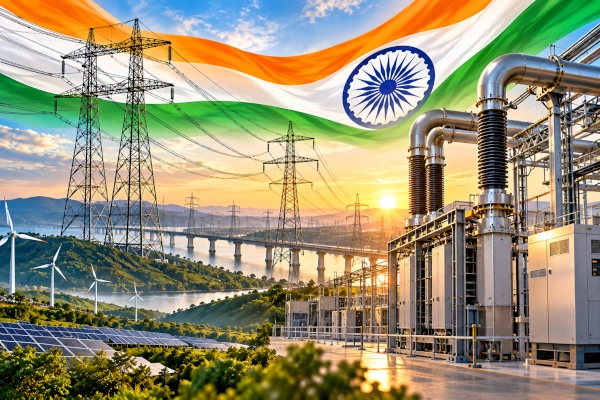
India is advancing a major initiative to develop indigenous silicon carbide (SiC) power semiconductor modules for high-voltage electricity transmission systems. Power Grid Corporation of India Limited (POWERGRID), the Ministry of Electronics and Information Technology (MeitY) and the Ministry of Power are jointly facilitating the development of advanced SiC MOSFET-based power modules for Voltage Source Converter–High Voltage Direct Current (VSC-HVDC) applications.
The programme aims to strengthen India’s capabilities in semiconductor design, fabrication, packaging, testing and integration into electricity transmission infrastructure. It will also support the development of intellectual property within India and reduce dependence on imported power semiconductor technologies used in strategically important grid applications.
As part of the initiative, MeitY has scheduled a stakeholder consultation on October 14, 2026, at Electronics Niketan in New Delhi, bringing together prospective technology developers and industry participants to discuss the programme’s technical and implementation requirements.
A major feature of the proposed programme is the development and validation of approximately 13,000 indigenous SiC power modules for pilot deployment in a 1,000 MW VSC-HVDC project. The initiative connects India’s expanding semiconductor ecosystem with its growing requirements for advanced electricity transmission infrastructure.
POWERGRID and MeitY Collaborate on Indigenous Power Semiconductor Development
The initiative brings together three important institutions involved in India’s technological and energy infrastructure development. MeitY will support the semiconductor technology programme, the Ministry of Power will provide the broader electricity sector framework, and POWERGRID will contribute its expertise in high-voltage transmission systems.
POWERGRID operates a major portion of India’s interstate electricity transmission infrastructure and has extensive experience in the development and operation of high-voltage transmission networks. Its participation will help connect semiconductor development with the technical requirements of utility-scale electricity transmission.
The programme covers the indigenous design, development, qualification, validation and pilot deployment of SiC MOSFET-based power modules. These modules are intended for use in advanced VSC-HVDC converter systems, which require sophisticated power electronics to control the transmission of large quantities of electrical energy.
By bringing semiconductor developers and transmission system specialists together, the initiative seeks to establish a pathway from technology development to practical use in India’s electricity network. The programme also supports the creation of domestic intellectual property and manufacturing expertise in a specialised category of high-power electronic devices.
Silicon Carbide Semiconductors Offer Advantages for Power Transmission
Silicon carbide is a semiconductor material increasingly used in power electronics because of its ability to operate under demanding electrical and thermal conditions. Compared with conventional silicon devices, suitably designed silicon carbide components can support higher operating voltages, faster switching and improved power conversion efficiency in selected applications.
These characteristics make SiC technology particularly relevant to electric vehicles, renewable energy systems, industrial equipment and advanced electricity transmission infrastructure.
A Metal-Oxide-Semiconductor Field-Effect Transistor, commonly known as a MOSFET, is an electronically controlled semiconductor switch. In power conversion systems, MOSFETs regulate electrical current by switching rapidly between conducting and non-conducting states.
Silicon carbide MOSFETs combine this switching function with the material advantages of SiC, making them suitable for increasingly demanding power electronic applications.
For high-voltage transmission, semiconductor switches are fundamental components of converters that control electrical energy flowing through the network. Developing suitable SiC modules requires careful engineering to achieve the necessary voltage ratings, current-handling capabilities, thermal performance and long-term reliability.
India’s proposed programme seeks to establish these capabilities domestically, creating opportunities for semiconductor designers, manufacturers and specialised engineering companies.
VSC-HVDC Technology Supports Advanced Electricity Transmission
High Voltage Direct Current transmission is used to move large quantities of electrical energy over long distances and to connect electricity networks under suitable operating conditions.
Unlike conventional alternating-current transmission, HVDC systems use converter stations to transform electrical power between alternating current and direct current. These systems can provide advantages for long-distance bulk power transmission, selected underground and submarine cable applications, and the interconnection of different electricity networks.
Voltage Source Converter technology represents an advanced approach to HVDC transmission. It uses controllable semiconductor switches to regulate power conversion and manage electrical energy flow.
VSC-HVDC systems are particularly relevant to modern electricity networks because they offer flexible control capabilities and can support the integration of renewable energy resources.
The semiconductor modules used in these converters must operate reliably under demanding electrical conditions. Their performance influences converter efficiency, thermal management and overall system reliability.
The development of indigenous SiC MOSFET modules will therefore strengthen India’s technological capabilities in an important component of modern power transmission infrastructure.
Indigenous Development Programme Targets 3.3 kV and 4.5 kV Semiconductor Modules
The programme establishes ambitious technical objectives for developing high-voltage silicon carbide power modules.
The initial target involves modules rated at 3,300 volts, with a maximum continuous drain current exceeding 1,800 amperes. These specifications reflect the high electrical demands associated with industrial-scale power conversion.
The initiative also includes a higher-voltage development target of 4,500 volts, with similar current-handling requirements. The technology platform is expected to support future development towards 6.5 kV device variants.
The modules will be developed for integration into HVDC converters, with attention to electrical insulation, switching performance, packaging and operational reliability.
According to the programme specifications, the module housing is expected to follow the IHM/IHV format, measuring approximately 190 × 140 millimetres. The design also targets an isolation voltage of 6 kV for one minute under the specified testing conditions.
These requirements create a technically demanding development programme that will require expertise in semiconductor device design, materials, fabrication, packaging and high-power electrical testing.
The objective is to develop a scalable domestic technology platform capable of supporting future requirements rather than producing a single specialised semiconductor component.
Programme Includes Pilot Procurement of Approximately 13,000 Modules
A significant feature of the initiative is its connection to an identified pilot application in India’s high-voltage transmission infrastructure.
The programme framework provides for the procurement of approximately 13,000 successfully validated SiC power modules for deployment in a proposed VSC-HVDC project.
The modules are intended for integration into converter equipment associated with an identified 1,000 MW pilot transmission application.
This arrangement provides a practical route for evaluating semiconductor technology under actual operating conditions.
Laboratory testing is essential during semiconductor development, but high-power grid applications also require extensive validation at equipment and system levels. Pilot deployment allows engineers to assess how developed components perform when integrated into operational converter infrastructure.
The proposed procurement arrangement also creates a potential commercial pathway for successful Indian semiconductor developers. By connecting research and development with a defined application, the programme seeks to encourage investment in manufacturing and qualification capabilities.
The pilot initiative is intended to establish the technical foundation for the wider use of indigenous semiconductor modules in future VSC-HVDC projects.
Indian Semiconductor Companies and Startups Can Participate
The programme is structured to encourage participation by Indian semiconductor companies, startups, micro, small and medium enterprises, and specialised technology developers.
Under the indicative eligibility framework, participating domestic companies must satisfy applicable Indian ownership and control requirements.
Companies may submit proposals independently or through consortium arrangements involving complementary technology and manufacturing partners.
The programme currently provides for consortium participation involving up to four organisations, including the lead applicant.
Academic institutions, national laboratories, research organisations and multinational companies may participate as consortium partners within the programme framework.
This approach recognises that developing high-voltage power semiconductor modules requires expertise across multiple disciplines. Semiconductor design companies may collaborate with fabrication facilities, packaging specialists, research institutions and organisations experienced in electrical testing.
Such partnerships can help India develop an integrated semiconductor manufacturing ecosystem extending beyond chip design into advanced power electronics production.
Development Programme Envisages 36-Month Technology Phase
The initiative proposes a development period of up to 36 months, followed by an additional period of up to six months for supplying qualified modules for pilot deployment.
The development process is structured around successive engineering and validation stages.
The first phase envisages the production of approximately 40–50 engineering samples within 18 months of the programme’s commencement. These samples will undergo preliminary design validation and switching tests to assess the performance of the proposed semiconductor architecture.
A subsequent development phase will involve design improvements and the production of additional near-production-ready samples. This stage is expected to culminate around the 33-month milestone.
Following successful module-level validation, the technology will undergo further testing at the converter valve level. These assessments will examine the suitability of the modules for integration into the intended VSC-HVDC equipment.
The programme will then proceed towards manufacturing qualified modules and their deployment in the identified pilot application.
This structured development process is intended to ensure that indigenous semiconductor technology meets the technical requirements associated with critical electricity transmission infrastructure.
Government Support to Encourage Domestic Semiconductor Innovation
The programme framework envisages financial support from MeitY to encourage indigenous semiconductor development.
Under the indicative guidelines, the ministry may support up to 50% of approved project costs, subject to the applicable scheme provisions and the final programme structure.
The proposal evaluation process is expected to place substantial emphasis on technical capability. The indicative framework assigns 70% weightage to technical evaluation and 30% to financial evaluation.
Prospective developers will need to demonstrate their ability to meet demanding semiconductor specifications while establishing credible arrangements for fabrication, packaging, testing and qualification.
The initiative also places importance on developing intellectual property within India.
Under the proposed framework, the principal design and development work for the indigenous HVDC SiC power modules must take place in India. The associated intellectual property should remain owned and effectively controlled by an Indian-incorporated company.
This approach supports the development of domestic technological capabilities while allowing collaboration with research institutions and industrial partners.
Stakeholder Consultation Scheduled in New Delhi on October 14
MeitY has scheduled a pre-Request for Proposal stakeholder consultation for October 14, 2026, between 2:30 PM and 4:30 PM.
The meeting will take place at Conference Room 1007, Electronics Niketan, CGO Complex, Lodhi Road, New Delhi.
The consultation is intended to bring together interested companies and technology developers to discuss the programme’s technical specifications, manufacturing requirements, development schedule and proposed implementation framework.
Participants will have an opportunity to provide feedback on semiconductor design capabilities, fabrication arrangements, qualification infrastructure and the feasibility of the proposed technical targets.
The exercise will also examine opportunities for collaboration between companies specialising in different stages of semiconductor development and manufacturing.
Following the consultation, MeitY intends to proceed with the detailed Request for Participation process. This will provide the framework for evaluating prospective developers and advancing the programme towards implementation.
The October 14 meeting represents an important preparatory step in developing India’s indigenous power semiconductor capabilities.
Indigenous SiC Modules Can Strengthen India’s Semiconductor Manufacturing Ecosystem
India has been expanding its semiconductor development initiatives through programmes supporting chip design, fabrication, assembly, testing and advanced electronics manufacturing.
The indigenous SiC power module initiative adds a specialised power electronics dimension to these efforts.
Power semiconductor devices differ from conventional processors and memory chips because they are designed primarily to control and convert electrical energy. Their applications extend across electric vehicles, renewable energy systems, industrial drives, railway traction and electricity transmission infrastructure.
Developing high-voltage SiC devices therefore creates opportunities for manufacturers operating in several strategically important sectors.
The proposed programme covers the complete semiconductor development chain, including device engineering, fabrication, module packaging, assembly, testing and system integration.
This integrated approach is particularly important because high-power semiconductor performance depends not only on the characteristics of the semiconductor material but also on packaging, electrical connections, thermal management and operational reliability.
By supporting domestic capabilities across these areas, the initiative can contribute to the development of a more comprehensive Indian power electronics manufacturing ecosystem.
Advanced Power Electronics Support India’s Expanding Electricity Grid
India’s electricity transmission infrastructure is expanding to accommodate increasing power demand, renewable energy generation and the development of new industrial centres.
High-voltage transmission systems play an important role in connecting generating stations with major consumption centres and supporting electricity movement between different regions.
Advanced converter technologies are becoming increasingly relevant as the power system incorporates greater quantities of renewable energy and develops more flexible transmission arrangements.
Semiconductor modules are critical components of these converter systems because they regulate electrical switching and power conversion.
Developing indigenous technologies for these applications can strengthen domestic engineering capabilities and support the long-term maintenance and development of strategic electricity infrastructure.
POWERGRID’s participation connects semiconductor research with practical transmission requirements, creating opportunities for technology developers to work towards clearly defined industrial applications.
POWERGRID Initiative Advances India’s Semiconductor and Energy Self-Reliance
The joint initiative involving POWERGRID, MeitY and the Ministry of Power marks an important step towards developing indigenous semiconductor technologies for India’s electricity transmission infrastructure.
The programme combines ambitious technical objectives with a practical development framework, including engineering samples, qualification testing and pilot deployment.
Its focus on 3.3 kV and 4.5 kV silicon carbide MOSFET modules addresses a specialised category of power electronics that is increasingly relevant to advanced transmission systems.
The proposed procurement of approximately 13,000 validated modules provides a pathway for moving successful technologies from development into practical grid applications.
The programme also encourages participation by Indian startups, semiconductor companies, research institutions and manufacturing partners, supporting the creation of domestic expertise across the semiconductor value chain.
By connecting India’s semiconductor development ambitions with the requirements of its electricity transmission network, the POWERGRID initiative strengthens the foundation for indigenous power electronics manufacturing. The programme represents an important contribution to Aatmanirbhar Bharat, the India Semiconductor Mission and the long-term development of a technologically advanced national power grid.
References
1. Ministry of Electronics and Information Technology, Government of India
Indigenous Design, Development, Qualification and Supply of SiC MOSFET Based Power Modules for Pilot Deployment in VSC-HVDC
Official Pre-RFP Stakeholder Consultation Programme
Stakeholder Consultation: October 14, 2026
https://c2s.gov.in/HVDC.jsp
2. Power Grid Corporation of India Limited — Official Announcement
Ministry of Power, Ministry of Electronics and Information Technology and POWERGRID Invite Expression of Interest for Indigenous Design and Development of SiC MOSFET-Based Power Semiconductor Modules for VSC-HVDC Systems
Published: September 25, 2026
https://www.powergrid.in/en/news
3. Power Grid Corporation of India Limited
Official information on India’s high-voltage electricity transmission infrastructure and HVDC systems.
https://www.powergrid.in/en/transmission
You may also like
-
Chennai Startup Evoxia Develops Hydrogen Plasma Technology for Indigenous Silicon Manufacturing
-
IIT Bombay Startup MumbaiSemi Develops Indigenous RF Chip Supporting India’s NavIC and Global Satellite Navigation Systems
-
Bengaluru Startup ImmunitoAI Uses Artificial Intelligence to Develop Next-Generation Antibody Medicines
-
Solar Defence Delivers Single Batch Supply of 450 Indigenous Nagastra-1R Loitering Munitions to Indian Army
-
Adani Enterprises and Jabil Announce 50:50 Joint Venture to Manufacture AI Servers and Data Centre Hardware in India
