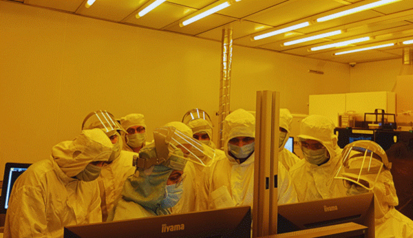
India’s semiconductor ambition is beginning to move beyond factories, incentives and investment announcements into the harder and more important terrain of human capability. A training initiative led by the Indian Institute of Science, Bengaluru, for tribal students has recorded a major expansion in participation during its 2026 Phase-II rollout, signalling that the country’s future chip ecosystem is also being built through wider social inclusion and grassroots technical exposure.
The programme is being implemented by IISc Bengaluru in collaboration with the Ministry of Tribal Affairs, with support from MY Bharat under the Department of Youth Affairs. It is coordinated through the Centre for Nano Science and Engineering at IISc, one of India’s important advanced research centres in nanotechnology and semiconductor-related fields. The aim is to expose tribal students and faculty members to semiconductor fabrication, nanoengineering processes and emerging technologies — areas that are central to India’s long-term technology workforce.
The most striking number is the jump in applications. Participation through MY Bharat youth networks rose from 992 applications in the previous phase to 5,654 applications in the current phase, marking a growth of 518%. That is not a small administrative increase; it shows a dramatic widening of awareness among students who may earlier have seen semiconductors as a distant or elite field.
The geographical spread is equally important. The programme expanded from 32 states to 34 states, while district participation rose from 411 districts to 648 districts. This means the initiative is reaching far beyond a few educational clusters and is beginning to touch students across a much wider national map. For a sector like semiconductors, where India needs talent across research, manufacturing, equipment handling, process engineering, testing, packaging and design support, such district-level expansion can become a valuable long-term foundation.
The data also carries a strong gender signal. Female participation increased from 268 applications in the previous phase to 1,741 applications in the current phase, a rise of more than 549%. This is one of the most encouraging aspects of the programme. Semiconductor careers are often seen through the lens of engineering campuses, laboratories and high-end manufacturing units. When tribal women begin entering this pipeline in greater numbers, it strengthens both STEM inclusion and India’s future technical workforce.
The structure of the programme is practical. It includes an online self-paced learning module, lectures by IISc faculty experts and a 10-day residential training programme at IISc Bengaluru. The residential component is especially important because it gives selected participants direct exposure to a premier scientific institution, laboratory culture, advanced equipment environments and expert-led academic mentoring. Free travel, lodging and food support also remove major financial barriers that could otherwise prevent eligible students from participating.
This is where the programme becomes more than a training exercise. For many first-generation learners, the biggest obstacle is not talent but access. A student from a tribal background may have the ability to understand advanced science, but may lack exposure to semiconductor labs, research mentors, national institutions and career pathways in emerging technologies. By bringing students into the IISc ecosystem, the initiative gives them a direct view of what high-end science looks like in practice.
The outreach model appears to have played a decisive role in the surge. MY Bharat field functionaries, State Directors, District Youth Officers and volunteer networks carried out mobilisation efforts across the country. The campaign also used virtual orientation sessions, coordination with technical universities and targeted awareness drives among tribal student communities. This is significant because awareness is often the first missing link in specialised technical programmes. Students cannot apply for opportunities they never hear about.
Technical institutions also helped expand the programme’s reach. Chhattisgarh Swami Vivekanand Technical University, for example, partnered in outreach efforts to engineering, polytechnic and pharmacy institutions. This kind of institutional networking matters because India’s semiconductor workforce will not come from one stream alone. It will require engineers, diploma holders, laboratory technicians, materials specialists, electronics graduates, process operators and faculty members who can carry knowledge back into regional institutions.
The wider timing of the initiative is important. India is trying to build a full semiconductor ecosystem, covering design, fabrication, assembly, testing, packaging, research and workforce development. Large plants and government incentives can create industrial capacity, but the sector cannot mature without trained people. Cleanroom discipline, wafer processing, nanoscale fabrication, materials science, quality control and device understanding require a steady pipeline of technically prepared youth. This programme addresses that need from an inclusion-first angle.
For tribal students, the value is also aspirational. Semiconductor technology is one of the most strategic sectors in the world today. Chips are used in mobile phones, electric vehicles, satellites, defence electronics, medical equipment, artificial intelligence systems, telecom networks and industrial automation. Exposure to this field gives students access to a career landscape linked to the future of global technology rather than only to conventional employment routes.
The inclusion of faculty members adds another layer of impact. When faculty from regional and tribal-serving institutions receive exposure to semiconductor fabrication and nanoengineering, the benefits can travel back into classrooms. A single trained teacher can influence hundreds of students over time. This multiplier effect can help improve technical awareness in institutions that may not yet have advanced semiconductor infrastructure of their own.
The programme also reflects a better understanding of how national missions must be built. India’s semiconductor push cannot remain limited to metropolitan research hubs and large corporate campuses. A genuine national ecosystem must connect premier institutions, state universities, polytechnics, youth networks, tribal communities and regional colleges. The IISc-led training programme shows how a high-technology mission can be widened without diluting its seriousness.
The growth in applications should also be read as a sign of changing ambition among young Indians. Tribal youth are responding to opportunities in frontier technology when the pathway is clearly communicated and logistical barriers are addressed. The numbers show that demand exists; the challenge now is to convert this demand into structured training, internships, advanced education, research opportunities and eventual employment.
The next stage will be crucial. A 10-day residential programme can open the door, but sustained impact will require follow-up modules, mentorship, certification, advanced training slots, industry exposure and links with India’s semiconductor projects. If the students who enter this programme are guided into internships, higher studies and technical jobs, the initiative can become a powerful feeder channel for India’s chip ecosystem.
At its heart, this initiative tells a larger story about India’s development model. The country is trying to enter one of the most advanced technology sectors in the world while also ensuring that historically underrepresented communities are not left watching from the margins. The surge from 992 to 5,654 applications is therefore more than a participation statistic. It is a signal that India’s semiconductor mission is beginning to acquire a social base.
The IISc-led programme brings together frontier science, youth mobilisation and tribal empowerment in a single frame. It gives India’s semiconductor journey a wider human foundation — one where cleanrooms, nanoengineering and chip fabrication are no longer distant ideas, but real possibilities for students from districts and communities that deserve a place in the country’s technology future.
You may also like
-
DGCA Introduces Training Framework for Gyroplane Pilots in India
-
DRDO CASDIC Opens 30 Paid Internships for Engineering and Science Students
-
Duryodhana Wins Shalya Through Hospitality: Gifts, Obligation and Political Leverage Before the Kurukshetra War
-
Krishna’s Private Meeting With Karna: Back-Channel Diplomacy Before the Kurukshetra War
-
One Voice – One Resolve – One India: Namami Bharatam Marks 150 Years of Vande Mataram Across the Nation
