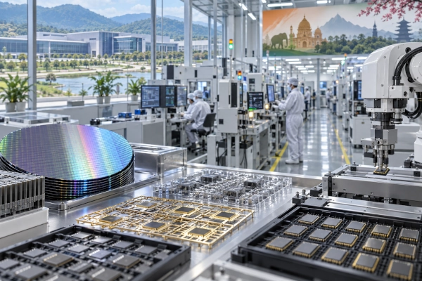
India’s semiconductor manufacturing ambitions have received another boost as Paras Semiconductors, a subsidiary of Paras Defence and Space Technologies Limited, advances its proposed ₹6,200 crore semiconductor packaging and testing project in Madhya Pradesh. The company has secured an allotment of 43 acres at Vikram Udyogpuri near Ujjain, according to information disclosed by the Madhya Pradesh Industrial Development Corporation.
The development was reported on 25 October 2026, following the conclusion of the Madhya Pradesh Semiconductor Summit 2026 in Indore. It represents a further step towards implementing the investment proposal formalised through a memorandum of understanding between Paras Semiconductors and the Madhya Pradesh government on 22 July 2026.
The proposed facility will focus on advanced semiconductor assembly, packaging and testing technologies, including specialised processes required for high-performance electronic components. The project is particularly relevant to India’s efforts to develop domestic semiconductor capabilities for defence, aerospace, telecommunications and other strategic applications.
The investment also reflects growing efforts to establish semiconductor-related manufacturing outside India’s traditional electronics and technology centres. Madhya Pradesh is seeking to develop the Indore-Ujjain region into an industrial corridor supporting chip design, advanced packaging, electronics manufacturing and related technological activities.
Paras Semiconductors Receives Land at Vikram Udyogpuri
The latest progress concerns the allotment of industrial land for the proposed semiconductor facility at Vikram Udyogpuri in the Ujjain region.
Rajesh Rathore, Executive Director of the Madhya Pradesh Industrial Development Corporation’s Ujjain office, confirmed that 43 acres had been allotted to Paras Semiconductors. The information emerged during reporting on the state’s semiconductor investment initiatives following the two-day summit in Indore.
The company’s original announcement on 22 July 2026 had referred to an allotment of 50 acres along the Ujjain-Indore Corridor. The latest reported figure of 43 acres therefore differs from the area mentioned in the original agreement announcement.
Both disclosures establish the project’s intended location within the Indore-Ujjain industrial region. However, the available information does not explain whether the difference reflects a subsequent adjustment to the land allocation or another administrative development.
Vikram Udyogpuri forms part of Madhya Pradesh’s industrial development efforts and provides an established location for attracting manufacturing investments. The proposed semiconductor project could contribute to the development of a broader industrial ecosystem involving specialised equipment suppliers, electronics manufacturers, engineering services and technology companies.
Land allocation represents an important preparatory milestone for a capital-intensive semiconductor project. The establishment of the facility will also require detailed engineering, specialised manufacturing equipment, utilities, technical infrastructure and a trained workforce before commercial operations can begin.
₹6,200 Crore Investment Proposal Formalised in July 2026
Paras Semiconductors signed a memorandum of understanding with the Madhya Pradesh government on 22 July 2026 to establish a greenfield advanced semiconductor facility in the Indore-Ujjain region.
The agreement involved the Department of Science and Technology of the Madhya Pradesh government, acting through the Madhya Pradesh State Electronics Development Corporation.
Under the proposed arrangement, the company and the state agency intend to combine their respective capabilities and institutional support to facilitate the development of the semiconductor project.
The investment proposal amounts to approximately ₹6,200 crore, making it a significant planned industrial project within Madhya Pradesh’s emerging semiconductor sector.
Paras Defence and Space Technologies disclosed the agreement to the stock exchanges under the applicable SEBI listing regulations, providing a formal record of the company’s proposed expansion into advanced semiconductor technologies.
The project remains at the development and implementation-planning stage. The investment figure represents the proposed project outlay and should not be interpreted as capital expenditure already completed.
The company intends to develop semiconductor capabilities that can support domestic demand for advanced electronic devices, particularly in applications requiring high performance, reliability and specialised functionality.
Understanding the Importance of Semiconductor Packaging and Testing
Semiconductor manufacturing involves several technically demanding stages, beginning with chip design and continuing through wafer fabrication, assembly, packaging, testing and integration into electronic systems.
A wafer fabrication plant produces semiconductor circuits on silicon or other suitable materials through complex processes involving lithography, deposition, etching and other manufacturing operations.
However, the completion of a silicon wafer does not immediately produce a chip ready for installation in an electronic device. Individual semiconductor dies must undergo further processing, protection, electrical connection and testing before they can function reliably within larger systems.
This is where outsourced semiconductor assembly and test facilities, commonly known as OSAT facilities, become important.
An OSAT facility undertakes semiconductor assembly, packaging and testing on behalf of chip designers, manufacturers and other customers. These activities form an essential part of the global semiconductor manufacturing value chain.
Packaging protects delicate semiconductor components from environmental and mechanical damage while providing the electrical connections required to communicate with external circuits.
Testing verifies whether the packaged devices meet specified functional, electrical and reliability requirements.
Advanced semiconductor packaging has become increasingly important as modern electronic systems require higher computing performance, improved power efficiency, greater component density and more sophisticated integration.
By developing domestic packaging and testing capabilities, India can expand its participation in semiconductor manufacturing without relying exclusively on the establishment of additional wafer fabrication plants.
Facility to Develop Advanced 2.5D and 3D Semiconductor Packaging
The proposed Paras Semiconductors facility will incorporate several advanced assembly and packaging technologies, according to the company’s July 2026 announcement.
These include 2.5D and 3D packaging, heterogeneous integration, hybrid bonding, ultra-high-density fan-out packaging, chiplet integration, wafer bumping, flip-chip assembly, and semiconductor testing and reliability assessment.
Each technology addresses different requirements associated with integrating increasingly complex semiconductor devices.
Traditional chip packaging generally involves mounting an individual semiconductor die inside a protective package and establishing electrical connections with external circuits.
Advanced packaging technologies go further by enabling multiple semiconductor components to operate together within highly integrated assemblies.
In 2.5D packaging, separate semiconductor dies can be positioned alongside one another and connected through an interposer or another high-density interconnection structure. This approach supports communication between components while reducing some limitations associated with conventional circuit-board connections.
Three-dimensional packaging enables semiconductor dies to be stacked vertically, improving integration density and potentially shortening electrical pathways between components.
Heterogeneous integration allows semiconductor devices manufactured using different technologies or optimised for different functions to be combined within a single package.
These capabilities are increasingly relevant to high-performance computing, advanced sensors, artificial intelligence processors and specialised electronic systems.
Chiplet Integration and Hybrid Bonding to Support High-Performance Electronics
Chiplet integration represents an important development in semiconductor architecture because it allows a complex electronic system to be constructed from multiple smaller semiconductor dies.
Instead of manufacturing every function within one large monolithic chip, designers can develop separate functional components and integrate them into a common package.
This approach can provide flexibility in selecting semiconductor manufacturing processes for different functions. Processing, memory, communication and specialised acceleration components can potentially use different technologies while operating together as an integrated system.
Hybrid bonding is another advanced technology identified in the Paras Semiconductors proposal.
It enables high-density connections between semiconductor surfaces and can support the integration of stacked devices with very fine interconnection structures.
Other proposed capabilities include wafer bumping and flip-chip assembly, which help establish electrical connections between semiconductor dies and their supporting substrates.
Ultra-high-density fan-out packaging can provide additional flexibility in arranging electrical connections while supporting compact electronic assemblies.
These are technically demanding manufacturing processes that require specialised equipment, cleanroom environments, precision engineering and rigorous quality-control procedures.
The inclusion of these technologies in the company’s project proposal indicates an ambition to participate in advanced semiconductor packaging rather than limit operations to conventional assembly processes.
Actual manufacturing capabilities will depend on the equipment installed, processes qualified and customer requirements addressed once the facility is developed.
Strategic Applications in Defence, Aerospace and Advanced Sensors
One of the distinctive aspects of the proposed investment is its connection with Paras Defence and Space Technologies, an Indian company operating in specialised defence and space engineering sectors.
Paras Semiconductors has identified strategic and high-performance sensor applications among the areas its advanced semiconductor capabilities are intended to support.
Modern defence and aerospace systems increasingly depend on sophisticated electronic components for sensing, communication, signal processing, navigation and information management.
Radar systems, electronic warfare equipment, electro-optical sensors, satellite payloads and advanced communication platforms require reliable semiconductor devices capable of meeting demanding operational specifications.
Semiconductor packaging can influence important device characteristics, including thermal management, electrical performance, mechanical reliability and resistance to environmental stress.
For applications requiring high reliability, the ability to test and qualify semiconductor assemblies becomes particularly important.
Domestic access to advanced packaging and testing services could create opportunities for Indian companies developing specialised defence and aerospace electronics.
However, a proposed semiconductor facility does not automatically establish qualification for military or space applications. Individual devices and manufacturing processes must meet the relevant technical, reliability and customer-specific requirements.
The strategic significance of the project lies in its potential contribution to India’s industrial capabilities across critical electronics technologies.
Madhya Pradesh Semiconductor Summit Attracts Investment Proposals
The latest information about the Paras Semiconductors project emerged as Madhya Pradesh concluded its two-day Semiconductor Summit 2026 in Indore on 24 October.
The summit brought together government representatives, technology companies, investors and industry specialists to explore opportunities in semiconductor manufacturing, advanced electronics and emerging technologies.
According to figures reported following the event, Madhya Pradesh received investment proposals exceeding ₹15,425 crore across semiconductor, electronics manufacturing and high-technology sectors.
The proposals were associated with expectations of more than 14,450 employment opportunities, although these figures represent projections rather than jobs already created.
Five companies received land-allotment letters covering proposed projects with investments totalling approximately ₹9,625 crore and an estimated potential for more than 4,450 direct jobs.
The summit also featured engagements involving businesses interested in chip design, electronics system design and manufacturing, semiconductor-related services and other advanced industrial activities.
Representatives from Japan, South Korea, Taiwan and Sweden participated in the event, reflecting the international dimensions of semiconductor supply chains and industrial cooperation.
The Madhya Pradesh government presented the summit as part of its efforts to establish the state as a destination for semiconductor-related investment and technological development.
Indore-Ujjain Corridor Identified for Semiconductor Development
The Madhya Pradesh government has identified the Indore-Ujjain Economic Corridor as an important location for developing semiconductor, electronics and advanced packaging industries.
The region benefits from its proximity to Indore, an established centre for education, commerce, manufacturing and information technology.
Industrial development along the corridor is intended to support new manufacturing facilities and encourage the growth of associated businesses.
Semiconductor packaging operations require a supporting network that extends beyond the principal manufacturing plant. Equipment maintenance, precision components, specialised chemicals, testing services, industrial utilities and trained technical personnel are all important parts of the ecosystem.
The establishment of multiple technology enterprises within a region can create opportunities for shared infrastructure, specialised service providers and closer collaboration between industry and educational institutions.
Madhya Pradesh is seeking to develop these capabilities through investment incentives, industrial land development and institutional partnerships.
The proposed Paras Semiconductors facility represents one component of this wider industrial strategy.
Its progress will be particularly important for assessing the state’s ability to translate semiconductor investment proposals into operational manufacturing capacity.
State Plans Semiconductor and Photonics Centres of Excellence
Alongside the investment announcements, Madhya Pradesh Chief Minister Mohan Yadav outlined plans to establish a Semiconductor Centre of Excellence and a Centre of Excellence for Photonics and Quantum Technologies.
These proposed institutions are intended to support research, innovation, technological development and workforce training.
Semiconductor manufacturing requires highly specialised skills covering electronics engineering, materials science, process engineering, equipment maintenance, quality assurance and industrial automation.
Advanced packaging introduces additional requirements involving precision assembly, thermal engineering, interconnection technology, reliability analysis and manufacturing process control.
Developing a trained workforce is therefore an important part of attracting semiconductor investments and supporting their long-term operation.
Photonics and quantum technologies also present opportunities for research and industrial development involving advanced sensors, optical systems, communications and specialised computing applications.
The proposed centres could support cooperation between educational institutions, research organisations and private companies.
Their effectiveness will depend on the establishment of suitable facilities, technical programmes, industry partnerships and sustained research activity.
Madhya Pradesh Semiconductor Policy Supports Industrial Investment
The state’s semiconductor development programme is supported by the Madhya Pradesh Semiconductor Policy 2025, which seeks to encourage investment in semiconductor manufacturing, chip design and associated industries.
The policy provides financial and administrative incentives for eligible projects, including capital expenditure support and assistance with industrial infrastructure.
According to the policy details reported during the summit, eligible semiconductor projects may receive incentives equivalent to 25% of eligible capital expenditure or 50% of applicable central government incentives, whichever is lower.
Additional provisions include support for certain semiconductor design activities, eligible stamp duty and registration expenses, interest subsidies and electricity-related incentives.
These measures are intended to reduce some of the financial and infrastructure challenges associated with establishing semiconductor operations.
Semiconductor packaging plants require substantial investment in specialised machinery, cleanroom systems, electricity supply, process utilities and quality-control infrastructure.
A supportive policy environment can improve the attractiveness of industrial locations, although investment decisions also depend on technical feasibility, market demand, customer relationships and access to skilled personnel.
The development of supporting industries and reliable infrastructure will remain important as Madhya Pradesh seeks to establish a competitive semiconductor manufacturing ecosystem.
India’s Semiconductor Mission Expands Beyond Wafer Fabrication
The Paras Semiconductors proposal forms part of a wider transformation underway in India’s electronics and semiconductor industries.
India’s semiconductor development strategy includes chip design, wafer fabrication, assembly, testing, packaging and the growth of supporting equipment and materials industries.
These activities are interdependent but require different technical capabilities and investment structures.
While wafer fabrication attracts considerable attention because of its technological complexity and capital requirements, assembly and testing facilities are equally important in converting semiconductor designs and fabricated dies into commercially usable components.
Advanced packaging has gained additional importance as device manufacturers seek improved performance through the integration of multiple semiconductor dies.
India’s growing electronics, telecommunications, automotive, aerospace and defence sectors provide potential demand for semiconductor products and associated services.
Domestic packaging and testing capacity could create opportunities for closer cooperation among Indian design companies, electronics manufacturers and semiconductor customers.
The proposed ₹6,200 crore facility in Madhya Pradesh is particularly relevant because it targets technologies associated with advanced integration and high-performance electronics.
Its development would add to India’s efforts to establish a more diversified semiconductor manufacturing ecosystem.
Paras Semiconductors Project Advances India’s Strategic Electronics Ambitions
The reported allotment of 43 acres at Vikram Udyogpuri marks further progress towards establishing Paras Semiconductors’ proposed advanced chip packaging and testing facility in Madhya Pradesh.
The project combines a substantial investment proposal with plans for technically sophisticated manufacturing processes, including 2.5D and 3D packaging, heterogeneous integration, chiplet assembly and advanced semiconductor testing.
Its association with Paras Defence and Space Technologies also provides a direct connection to India’s strategic electronics and high-performance sensor industries.
At the state level, the investment proposal complements Madhya Pradesh’s efforts to develop the Indore-Ujjain region into a centre for semiconductor manufacturing, chip design and advanced industrial technology.
The next stages will involve translating the proposed investment and land allocation into manufacturing infrastructure, qualified production processes and commercial capabilities.
The continuing development of such projects reflects India’s expanding participation in semiconductor technologies beyond conventional electronics assembly.
As domestic companies pursue advanced manufacturing capabilities and state governments strengthen industrial infrastructure, projects such as the proposed Paras Semiconductors facility can contribute to a broader foundation for India’s technological self-reliance, industrial innovation and strategic electronics development.
References
- Paras Defence and Space Technologies Limited, 22 July 2026. Stock-exchange disclosure and press release titled Government of Madhya Pradesh and Paras Semiconductors Sign MoU for ₹6,200 Crore Semiconductor Facility. Primary company announcement detailing the proposed investment, semiconductor technologies and originally announced 50-acre allotment.
- Business Standard, 25 October 2026. MP Semicon Summit Draws ₹15,425 Crore Investment Proposals, 14,000 Jobs in Sight. Reporting on the Indore summit and confirmation from Madhya Pradesh Industrial Development Corporation Executive Director Rajesh Rathore regarding the 43-acre allotment at Vikram Udyogpuri.
- Business Standard, 22 July 2026. Paras Semiconductors Signs MoU with MP State Electronics Development Corporation. Details of the proposed greenfield OSAT facility and advanced packaging technologies.
- ETGovernment, 22 July 2026. MP Government, Paras Semiconductors Sign MoU for ₹6,200 Crore OSAT Facility on Ujjain-Indore Corridor. Background on the investment proposal and semiconductor development plans.
- Madhya Pradesh Government, 23–24 October 2026. Announcements associated with Madhya Pradesh Semiconductor Summit 2026, Indore. Information concerning proposed investments, industrial development, technical education and centres of excellence.
- Madhya Pradesh Semiconductor Policy 2025. State government policy framework governing incentives and support measures for eligible semiconductor manufacturing and design projects.
- Ministry of Electronics and Information Technology, Government of India. India Semiconductor Mission. National policy framework for strengthening semiconductor design, manufacturing, assembly, testing and packaging capabilities.
You may also like
-
CSIR-CRRI Partners with Industry to Develop Advanced Indigenous Airport Runway and Pavement Materials
-
Petronet LNG Plans ₹1,200 Crore Joint Venture for Ten Compressed Biogas Plants Across India
-
India Seeks South Korean Shipbuilding Partnerships as Sarbananda Sonowal Begins Four-Day Visit to Busan
-
Koraput Kalajeera Rice of Odisha: The GI-Tagged Aromatic Heritage of India’s Ancient Rice-Growing Region
-
ICAR Scientists Develop Indigenous Protective Gloves for Cotton Farmers, Sign Commercial Manufacturing Agreement
