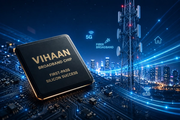
India’s domestic semiconductor design programme has recorded another significant milestone, with Chennai-based Aheesa Digital Innovations achieving first-pass silicon success for VIHAAN, an indigenous networking System-on-Chip designed specifically for fibre broadband applications.
The Ministry of Electronics and Information Technology (MeitY) announced the achievement on August 15, 2026. Aheesa had completed the VIHAAN tape-out on Republic Day, January 26, 2026, before reaching the first-pass silicon milestone on Independence Day. The company will now take the chip through further development and validation, with a production tape-out targeted for 2027.
The development is particularly notable because VIHAAN combines an Indian-designed broadband networking SoC with the indigenous VEGA microprocessor developed by C-DAC, bringing together technologies created within India’s growing semiconductor ecosystem.
What Is VIHAAN?
VIHAAN is being developed as a networking processor for fibre broadband equipment that connects homes and businesses to high-speed optical networks.
Earlier information released by the government described VIHAAN as a Gigabit Passive Optical Network, or GPON, Optical Network Terminal and networking SoC built around the indigenous VEGA processor. The chip integrates functions associated with fibre termination, data processing and network management into a common semiconductor platform.
A previous MeitY roadmap also disclosed more technical details about the platform. VIHAAN uses a 64-bit C-DAC RISC-V-based VEGA processor and incorporates security capabilities including Secure Boot. The design also supports interfaces required by modern networking equipment, including PCIe 3.0 and USB 3.0.
This positions VIHAAN for equipment such as fibre broadband gateways, optical network terminals and other customer-premises networking products.
For India, such equipment has strategic significance because broadband infrastructure is expanding rapidly through fibre deployment, 5G backhaul and increasingly data-intensive digital services. Domestic access to the underlying networking silicon can therefore reduce dependence on imported chip designs while giving Indian equipment manufacturers greater control over future products.
What First-Pass Silicon Success Means
A semiconductor project moves through several stages before reaching commercial production. Engineers first develop and verify the design before completing a tape-out, when the final design data is sent for fabrication.
The resulting physical chips then undergo extensive testing to determine whether the design behaves as expected.
Achieving first-pass silicon therefore represents an important engineering milestone because the initial fabricated version has successfully progressed through silicon validation without requiring the design team to begin again with a fundamental redesign.
However, first-pass silicon should not be confused with the start of mass production. Aheesa still has to move VIHAAN through further validation, productisation, customer testing and the production tape-out process before commercial volume deployment.
MeitY says VIHAAN is now moving towards that next stage, with production tape-out planned for 2027.
Built Around India’s VEGA Processor
One of VIHAAN’s most important characteristics is its use of the VEGA processor developed by the Centre for Development of Advanced Computing, C-DAC.
VEGA is based on the RISC-V instruction-set architecture, an open-standard processor architecture that is increasingly being adopted for embedded, industrial and specialised computing applications.
Building a commercial networking SoC around an indigenous processor is important because semiconductor self-reliance extends beyond manufacturing wafers. Processor architecture, intellectual property, chip design, verification, security features and the software ecosystem all form important parts of the semiconductor value chain.
VIHAAN consequently represents the integration of an Indian processor technology into a chip intended for a practical commercial telecommunications application rather than remaining limited to an experimental platform.
Government’s DLI Programme Supports Aheesa
Aheesa is among the companies supported under the government’s Design Linked Incentive Scheme, which aims to help Indian semiconductor companies move from chip concepts to commercially deployable products.
MeitY says chip design can contribute as much as 50% of the value addition in the semiconductor value chain and can account for around 15% to 35% of the bill-of-material cost of electronic products.
That makes design intellectual property an important area for India even as the country builds domestic fabrication and packaging capacity.
The DLI programme currently supports chip development for applications including satellite communications, drones, defence and aerospace systems, surveillance equipment, automobiles, AI, Internet of Things devices, telecom equipment, LED drivers and smart meters.
Aheesa also received substantial private and state-backed financial support. According to MeitY, the company raised around ₹40 crore earlier in 2026 from the Tamil Nadu Infrastructure Fund Management Corporation through the Tamil Nadu Emerging Sector Seed Fund, along with other private investors. The funding is intended to support product development and the company’s expansion.
Indian Chip Designs Moving Into Silicon
VIHAAN forms part of a broader wave of semiconductor projects now progressing from design files into physical silicon.
MeitY says companies supported by the DLI programme have completed more than 30 chip design tape-outs across different semiconductor foundries and have collectively attracted over $100 million in venture-capital funding. The government’s August 15 announcement puts the cumulative figure at 35 design tape-outs.
The government has also expanded access to advanced semiconductor design tools. State-of-the-art chip-design tools have been made available to 455 organisations, including 350 academic institutions and 105 startups.
Meanwhile, the Chips to Startup programme has enabled 71 academic institutions to complete 245 chip-design tape-outs, helping develop a larger pool of engineers with practical semiconductor-design experience.
These measures address an important part of the semiconductor challenge: producing engineers who understand not only circuit theory but the complete process of design, verification, tape-out and silicon testing.
Other Indian Semiconductor Startups Reach Key Milestones
VIHAAN is not an isolated project.
MeitY says Vervesemi Microelectronics has achieved first-pass silicon success for a BLDC motor-controller chip using an indigenous processor from InCore Semiconductor, along with its motor-driver chip.
Netrasemi has successfully tested a 12-nanometre Vision SoC with integrated video-analytics acceleration, while OptoML has received its 12-nm compute-in-memory SoC aimed at accelerating AI workloads while improving energy efficiency.
Mindgrove Technologies has partnered with PRAMA India to explore the use of its Vision SoC in CCTV surveillance cameras, while IndieSemiC has secured global certification for its Bluetooth BLE 6 chip module.
Together, these programmes show that India’s semiconductor effort is beginning to move beyond design proposals towards fabricated, tested and application-focused devices.
Semicon 2.0 Expands the Programme
India’s semiconductor programme received another major boost in July 2026 when the Union Cabinet approved Semicon 2.0 with an outlay of ₹1,27,500 crore.
The programme covers six broad areas: semiconductor design, machines and materials, additional fabrication facilities, expansion of ATMP and OSAT packaging capacity, research and development, and semiconductor talent.
Under the first phase of the India Semiconductor Mission, the government has approved 12 semiconductor manufacturing projects involving cumulative investment exceeding ₹1.64 lakh crore.
These include a silicon fab, a silicon-carbide fab, an integrated Gallium Nitride Micro-LED display facility and nine semiconductor packaging units.
The government says Micron, Kaynes and CG Semi have begun commercial production, while another approved project is expected to commence production during 2026. Importantly, the Cabinet’s Semicon 2.0 announcement states that India’s first semiconductor fab is scheduled to be commissioned in 2028.
This distinction matters because semiconductor packaging and assembly facilities are already entering production in India, while large-scale domestic wafer fabrication is still being built.
VIHAAN Connects Indigenous Design With a Commercial Application
The significance of VIHAAN lies not merely in producing another prototype chip. It demonstrates how several parts of India’s semiconductor strategy can come together in a single product.
An Indian fabless company has designed the networking SoC. The processor at its core comes from India’s C-DAC VEGA programme. Government incentives have supported the design process, while private and state-backed investors have supplied additional capital.
The next challenge will be to convert successful silicon into a product that equipment manufacturers can qualify, purchase and deploy at scale.
If VIHAAN successfully completes that transition, India would gain a domestically designed semiconductor platform for an important segment of its expanding broadband infrastructure.
It would also demonstrate a larger shift in the country’s semiconductor ambitions: from having Indian engineers participate predominantly in global chip-design programmes to building Indian semiconductor intellectual property, Indian processors and Indian-designed commercial SoCs intended for domestic as well as international markets.
Sources
Ministry of Electronics & IT / Press Information Bureau — August 15, 2026: Official announcement confirming Aheesa Digital Innovations’ first-pass silicon success with VIHAAN, its DLI support, ₹40-crore funding, 2027 production tape-out target and wider DLI ecosystem milestones.
Ministry of Electronics & IT / PIB — January 4, 2026: Government backgrounder describing VIHAAN’s GPON broadband architecture and integration with the indigenous VEGA processor.
Ministry of Electronics & IT / PIB — September 4, 2025: Government semiconductor roadmap detailing VIHAAN’s 64-bit C-DAC VEGA processor, Secure Boot and networking interfaces.
Union Cabinet / PIB — July 15, 2026: Official Semicon 2.0 approval detailing the ₹1,27,500-crore outlay, 12 approved manufacturing projects and roadmap for additional semiconductor fabs.
You may also like
-
Astra Microwave Expands Counter-Drone Capabilities with Layered Detection and Neutralisation Systems
-
MDL Begins Development of Indigenous Lithium-Ion Battery System for Project-75(I) Submarines
-
Tarang Shakti Delegates from 28 Countries Visit HAL and BEL to Explore India’s Defence Manufacturing Ecosystem
-
India’s 114 Rafale Fighter Jet Programme Moves Towards Final Decision with Focus on Indigenous Integration
-
Embraer and Mahindra Identify Nagpur as Potential C-390 Millennium Assembly Hub in India
