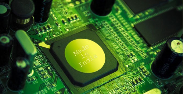
India has made significant progress toward building a skilled semiconductor workforce under the Chips to Startups (C2S) initiative, a key component of the India Semiconductor Mission aimed at strengthening the country’s technological capabilities and semiconductor ecosystem.
According to Union Minister for Railways, Information & Broadcasting and Electronics & IT Ashwini Vaishnaw, the country has already achieved notable progress toward its 10-year target of training 85,000 engineers in semiconductor design. The initiative focuses on talent development through training, upskilling and workforce development programmes across academic institutions nationwide.
Expanding Semiconductor Education Across India
At present, 315 academic institutions across the country are participating in the programme, enabling students from Assam to Gujarat and from Kashmir to Kanyakumari to gain hands-on experience in semiconductor technologies.
Through the programme, students are being trained in various stages of chip development, including:
- Semiconductor design
- Chip fabrication
- Packaging
- Testing
To support this training ecosystem, leading global technology companies such as Synopsys, Cadence Design Systems, Siemens, Renesas Electronics, Ansys, and Advanced Micro Devices have provided world-class Electronic Design Automation (EDA) tools to participating institutions.
These tools allow students to design semiconductor chips using industry-standard software. The designed chips are then fabricated and tested at the Semiconductor Laboratory in Mohali, giving learners exposure to the entire chip development cycle—from design to fabrication, packaging and testing.
World’s Largest Open-Access EDA Programme
The initiative has evolved into what the government describes as the world’s largest open-access Electronic Design Automation programme. So far, students and researchers have recorded more than 1.85 crore hours of EDA tool usage for chip design training.
This hands-on exposure is enabling young engineers to develop industry-relevant skills and contribute to India’s emerging semiconductor ecosystem.
Rising Global Demand for Semiconductor Talent
Highlighting future industry opportunities, Minister Vaishnaw noted that the global semiconductor industry is expected to expand from its current size of USD 800–900 billion to nearly USD 2 trillion in the coming years.
Such rapid growth is projected to create demand for nearly two million skilled professionals worldwide, presenting significant employment opportunities for India’s youth and technology workforce.
Expansion Under India Semiconductor Mission 2.0
Looking ahead, the government plans to expand the programme under India Semiconductor Mission 2.0. The initiative will extend participation from the current 315 academic institutions to 500 institutions across the country.
This expansion aims to ensure a steady pipeline of highly trained engineers capable of working in semiconductor design, fabrication, packaging and testing, thereby strengthening India’s domestic capabilities in the sector.
Building a Self-Reliant Semiconductor Ecosystem
Reiterating the government’s vision, Minister Vaishnaw stated that India is committed to building a robust and self-reliant semiconductor ecosystem through strategic investments in talent development, infrastructure creation and industry partnerships.
With initiatives such as the Chips to Startups programme and India Semiconductor Mission 2.0, the country aims to position itself as a global hub for semiconductor innovation and manufacturing in the coming decade.
Refernce: PIB
You may also like
-
India’s Golden Sweep at the 56th International Physics Olympiad 2026 held at Bucaramanga, Colombia
-
IIM Bangalore’s Indonesia Campus: India Takes Its Management Education to Southeast Asia
-
Digital India at 11: Over 110 Crore Academic Records Digitised, Making Education Services Faster and Paperless
-
Gurukul Diplomacy in Vienna: Indian Envoy Brings Panchatantra Tales to Austrian Children
-
Chanakya in the Age of Hormuz