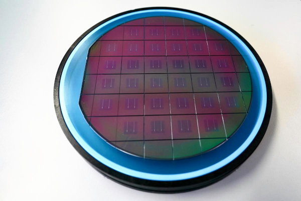
Scientists from Jawaharlal Nehru Centre for Advanced Scientific Research (JNCASR), an autonomous institute under the Department of Science and Technology, have fabricated an economical and energy-efficient wafer-scale photodetector (thin slice-based) using gold – silicon interface, for security applications.It could help detect weak scattered light as an indication of unwanted activity.
Photodetectors are the heart of any optoelectronic circuit that can detect light and are employed for a wide variety of applications ranging from controlling automatic lighting in supermarkets to detecting radiation from outer galaxy as well as security-related applications. However, the material cost and the intricate fabrication processes involved in realizing high-performance detectors make them unaffordable for day to day applications.
The invention by JNCASR scientists,which was published in the journal Applied Electronic Materials of the American Chemical Society, provides a simple and cost-effective solution-based fabrication method for high-performance photodetector.
The scientists have fabricated gold (Au)– silicon (n-Si) interface, which showed high sensitivity towards light demonstrating the photodetection action. The Au–Si interface was brought about by galvanic deposition, a technique for electroplating of metals, wherein water-based solutions (electrolytes) are used, which contain the metals to be deposited as ions. In addition,a nanostructured Au film also was deposited on top of p-type silicide (having an excess of positive charges), which acts as a charge collector.
Being a solution-based technique, the method is highly economical and enabled large-area fabrication without compromising the detector response. The process is quick, taking only minutes to fabricate a detector of any arbitrary area. The metal nanostructures enhanced the performance of the fabricated detector through trapping the incoming light. This photodetector displayed long-term environmental stability.
The detector exhibits a rapid response of 40microseconds and can detect low light intensities. The device covers a broad spectral range from Ultraviolet to Infrared.Besides, it shows excellent uniformity throughout the entire active area with less than 5% variation in response. Notably, the detector operates in self-powered mode, which means the device does not require external power for its operation, thus making it energy efficient. With a commonly available protective coating, excellent environmental stability is shown for the device under the harsh conditions for several days. The scientists also demonstrated the photodetector’s utility as a prototype imaging system, lux and power meter, and also as a tool for security applications.
Source: PIB
Image Courtesy:FibreSystems
You may also like
-
Indian Scientists Rewrite a 50-Year-Old Rule of Bacterial Gene Regulation
-
MeitY Unveils Indigenous 30 kW WBG-Based Integrated Drive System to Power India’s EV Revolution
-
CeNS Researchers Unlock Enhanced Optical Performance with Gold–LC Composite
-
Sarvam AI: Powering a Made-in-India AI Revolution
-
Csir-ampri Designed & Developed Sodar System Facility Inaugurated At IMD
